
On this page
The CBSE 2026-27 sample paper for Class 12 physics has two case study-based questions of four marks each in Section D, and one of them is on semiconductors. Calculators are not allowed, so every number below works by hand. Here are three original cases on the current NCERT Chapter 14, Semiconductor Electronics, easiest first. For the full chapter plan, read our semiconductor electronics Class 12 board exam guide.
Case 1: What happens to holes when a wafer is doped?
A sensor start-up in Bengaluru buys pure silicon wafers. At the lab's temperature, the datasheet gives the intrinsic carrier concentration as nᵢ = 1.0 × 10¹⁶ m⁻³. The team dopes one wafer with phosphorus at 2.0 × 10²¹ atoms m⁻³, and every donor atom gives up its extra electron. The wafer now conducts far better than the pure sample. During a reliability test, the wafer is warmed until nᵢ rises to 4.0 × 10¹⁶ m⁻³. An intern worries that the warm wafer might stop behaving as the same type of semiconductor.
(i) The doped wafer is: (a) p-type, holes in majority (b) n-type, electrons in majority (c) intrinsic (d) n-type, holes in majority
(ii) Name one other dopant that would make the same type of semiconductor from silicon.
(iii) Find the hole concentration in the doped wafer at the lab temperature.
(iv) Find the hole concentration in the warm wafer and say whether the intern's worry is justified.
Answers.
(i) (b). Phosphorus is pentavalent, so it donates an electron and electrons become the majority carriers.
(ii) Arsenic or antimony, pentavalent donors listed in NCERT Section 14.4.
(iii) nₑ ≈ 2.0 × 10²¹ m⁻³, so nₕ = nᵢ²/nₑ = (1.0 × 10³²)/(2.0 × 10²¹) = 5.0 × 10¹⁰ m⁻³.
(iv) nₕ = (1.6 × 10³³)/(2.0 × 10²¹) = 8.0 × 10¹¹ m⁻³, 16 times more. Electrons from donors do not depend on temperature, so nₑ stays near 2.0 × 10²¹ m⁻³ and the wafer is still n-type. The worry is not justified.
Case 2: How do you read a diode's I-V table?
For her practical file, Meera in a Kolkata school measures a silicon diode. In forward bias, her milliammeter reads 0.1 mA at 0.50 V, 0.6 mA at 0.60 V, 5 mA at 0.70 V, 13 mA at 0.75 V and 31 mA at 0.80 V. She then reverses the battery and switches to a microammeter. It reads 1.8 µA at −4 V and only 2.0 µA at −12 V. Her lab partner expected the reverse current to triple when the voltage tripled.
(i) She changed meters because: (a) the reverse current is far smaller than the forward current (b) the diode heats up in reverse bias (c) a milliammeter cannot read negative values (d) the reverse current is larger
(ii) Estimate the cut-in voltage of this diode from her table.
(iii) Find the dynamic resistance between 0.75 V and 0.80 V.
(iv) Find the diode's reverse resistance at −12 V and explain why the current barely changed from −4 V to −12 V.
Answers.
(i) (a). Forward current is in mA; reverse current is in µA.
(ii) About 0.7 V: below it the current is tiny, above it the current rises steeply, matching NCERT's ~0.7 V for silicon.
(iii) r_d = ΔV/ΔI = 0.05 V/(18 × 10⁻³ A) ≈ 2.8 Ω.
(iv) R = 12 V/(2.0 × 10⁻⁶ A) = 6.0 × 10⁶ Ω. Reverse current is the drift of minority carriers across the junction; even a small voltage sweeps all of them across, so the current is limited by their number, not by the voltage.
Case 3: Why does a bigger capacitor give steadier dc?
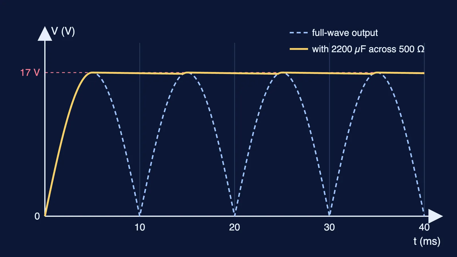
A repair shop in Ludhiana builds a bench power supply. A transformer gives 12 V rms between each end of its secondary and the centre tap, feeding two diodes D1 and D2 in a full-wave rectifier. The load is 500 Ω. On a CRO the technician sees half-sine pulses exactly 10 ms apart. She then adds a capacitor across the load and must choose between 100 µF and 2200 µF. Treat the diodes as ideal.
(i) The ac input frequency is: (a) 25 Hz (b) 50 Hz (c) 100 Hz (d) 200 Hz
(ii) If D2 burns out and stops conducting, how far apart are the pulses now?
(iii) What is the peak voltage across the capacitor with no load attached?
(iv) Which capacitor gives the steadier output, and why?
Answers.
(i) (b). A full-wave rectifier gives one pulse per half-cycle, so the period is 20 ms and the frequency 50 Hz.
(ii) 20 ms. Only D1 conducts, so the circuit acts as a half-wave rectifier, one pulse per cycle.
(iii) Each diode rectifies only half the secondary, 12 V rms. Peak = 12√2 ≈ 17 V, and an unloaded capacitor stays charged to this peak. (A real silicon diode drops about 0.7 V, giving about 16.3 V.)
(iv) 2200 µF. Between pulses the capacitor discharges through the load, and its voltage falls at a rate that depends inversely on the time constant CR (NCERT Section 14.7). With the same 500 Ω load, the larger capacitor gives a much larger time constant, so the voltage falls less before the next pulse recharges it and the output stays nearer the 17 V peak.
How to attack case-study questions
For general strategy, see our guide to answering case-based questions in board exams. For this chapter:
Name the carrier first. Decide n-type or p-type, then which carriers are majority, before any calculation.
Use nₑnₕ = nᵢ² with powers of ten. Square nᵢ, divide by the majority concentration, and check the minority count is far smaller.
Read I-V data by region. Cut-in, steep forward rise, flat reverse current: each part of the table answers a different sub-question.
Track pulses, not just frequency. Full-wave doubles the pulse rate; a dead diode halves it.
Test yourself on the reasoning. Our assertion-reason questions on semiconductor devices drill the same ideas, and the Fermi Problem Library has worked problems with a step-by-step solver that explains the reasoning rather than printing an answer.