
On this page
In the CBSE Class XII Physics curriculum for 2026-27, the theory marks table prints 7 (out of 70) in a cell of its own for Unit–IX Electronic Devices, which holds one chapter: "Chapter–14: Semiconductor Electronics: Materials, Devices and Simple Circuits". In the 2026-27 sample paper, the unit is Q22 (3 marks) and the Q29 case study (four 1-mark parts). Our semiconductors guide for JEE Main covers JEE; this post is about boards.
What does the semiconductor syllabus include for 2026-27?
CBSE lists energy bands in conductors, semiconductors and insulators (qualitative ideas only), intrinsic and extrinsic semiconductors (p and n type), the p-n junction, diode I-V characteristics in forward and reverse bias, and the diode as a rectifier. CBSE's note adds that content marked in NCERT textbooks as excluded for 2026-27 is not to be tested by schools.
The NCERT Chapter 14 file (pages stamped Reprint 2025-26) already matches this list: it ends at Section 14.7, the rectifier, with six exercises, and has no transistor, Zener diode, LED, solar cell or logic-gate sections. Revise only what it keeps:
Bands: insulators Eg > 3 eV, semiconductors Eg < 3 eV; diamond 5.4 eV, Si 1.1 eV, Ge 0.7 eV, and Sn 0 eV, a metal.
Intrinsic: ne = nh = ni, and I = Ie + Ih.
Extrinsic: donors (As, Sb, P) give n-type, ne >> nh; acceptors (In, B, Al) give p-type, nh >> ne; ne nh = ni² always, and the crystal stays neutral.
Junction: diffusion and drift balance; the depletion region is about one-tenth of a micrometre thick.
Diode: barrier V0 − V in forward bias, V0 + V in reverse; cut-in about 0.7 V (Si) and 0.2 V (Ge); rd = ΔV/ΔI.
Rectifiers: half-wave, full-wave with a centre-tap transformer, and the capacitor filter.
What do board questions on semiconductors look like?
Sample paper Q22 asks you to compare the band diagrams of metals, insulators and semiconductors, explain how band gap decides conductivity, and say why diamond insulates while tin conducts. The marking scheme gives three 1-mark points: metals and insulators together, semiconductors, and the diamond-tin reasoning. Q29, a polymer-semiconductor case study, asks why semiconductors suit wearable devices, then tests band gaps, intrinsic carriers, and majority and minority carriers. Calculators are not allowed.
Diagrams to practise until you can draw them from memory:
Three band diagrams with EC, EV and Eg labelled.
A p-n junction with fixed ions in the depletion region.
The I-V curve in both quadrants: forward current in mA rising after the knee, reverse current in µA almost flat.
Half-wave and full-wave circuits with input and output waveforms.
Worked example: a half-wave rectifier with a real diode
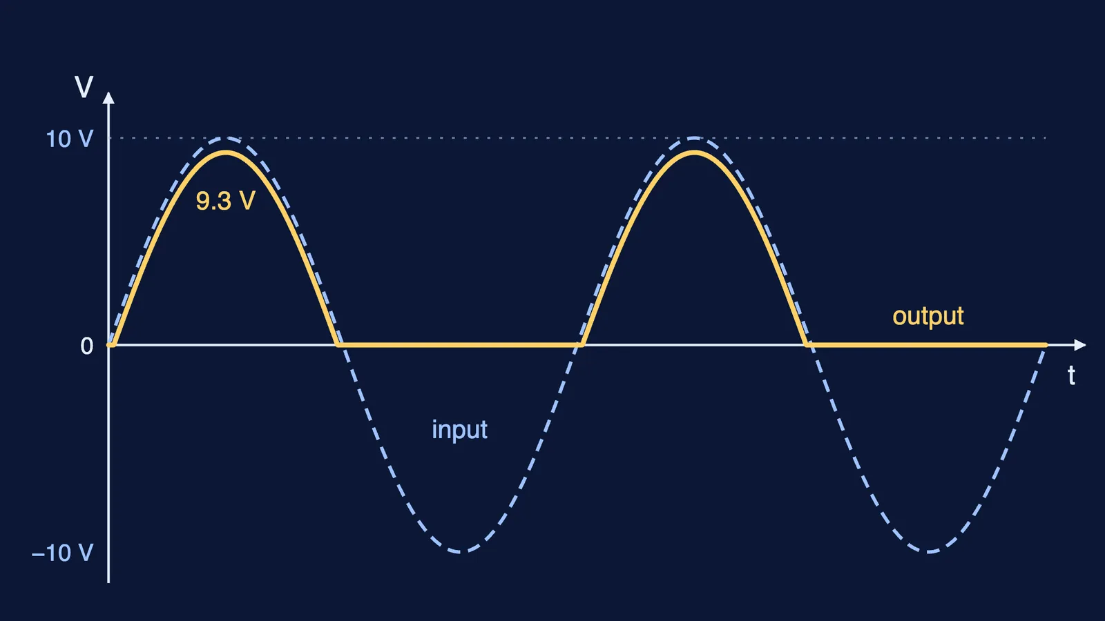
A silicon diode and a 1 kΩ load are in series across a transformer secondary giving 10 V peak at 50 Hz. Treat the diode as a fixed 0.7 V drop once it conducts, and as open below that and in reverse. Find (a) the peak output voltage, (b) the peak current, (c) when in each cycle the diode conducts, (d) the reverse voltage it must withstand.
Peak output: 10 − 0.7 = 9.3 V.
Peak current: 9.3 V ÷ 1000 Ω = 9.3 mA.
Conduction starts when 10 sin ωt = 0.7, so sin ωt = 0.07. For a small angle, ωt ≈ 0.07 rad (about 4°). With ω = 2π × 50 ≈ 314 rad/s, t ≈ 0.07 ÷ 314 ≈ 0.22 ms. By symmetry it stops 0.22 ms before 10 ms, so it conducts from 0.22 ms to 9.78 ms of every 20 ms: a little under half the cycle.
In the negative half the diode blocks the full 10 V. NCERT says breakdown voltage must be sufficiently higher than the peak secondary voltage, so pick a rating well above 10 V.
The image at the top plots this input and output.
Which mistakes cost marks?
Free carriers in the depletion region. It holds immobile ionised donors and acceptors.
Reversed forward bias. The p-side goes to the positive terminal.
Calling p-type material positively charged. It is neutral overall.
ED and EA misplaced. ED sits just below EC; EA just above EV.
Saying doping raises both carriers. Minority carriers fall, because ne nh = ni².
How should you revise Semiconductor Electronics in 7 days?
Day 1: the three band diagrams, from memory.
Day 2: intrinsic and extrinsic, with two ne nh = ni² numericals of your own.
Day 3: junction formation.
Day 4: biasing and the I-V curve with both scales.
Day 5: rectifiers and filter; redo the worked example with 15 V peak.
Day 6: sample paper Q22 and Q29, timed, marked against the scheme.
Day 7: NCERT Exercises 14.1 to 14.6 and every diagram once more.
If a numerical keeps failing at one step, the Fermi Problem Library has worked problems with a step-by-step solver that explains the reasoning rather than printing an answer.
Next, read our Dual Nature of Radiation and Matter board guide and our Nuclei board guide.