
On this page
Semiconductor questions in JEE Main return to a few ideas: carriers, bias, rectifier frequency, Zener regulation and gate circuits. Below: the syllabus, worked circuits and a one-week plan.
What does the JEE Main 2027 syllabus include for semiconductors?
The NTA's Syllabus for JEE (Main) - 2027 lists, under Electronic Devices: semiconductors, diode I-V characteristics in forward and reverse bias, the diode as a rectifier, I-V characteristics of the LED, photodiode, solar cell and Zener diode, the Zener diode as a voltage regulator, and logic gates (OR, AND, NOT, NAND and NOR). Transistors are not listed.
The current NCERT Semiconductor Electronics chapter stops at the rectifier, with no Zener diode, LED, photodiode, solar cell or logic gates. Learn bands, doping, the junction and rectifiers there. For the Zener diode and gates, use a second source such as the NIOS lesson on applications of semiconductor devices; for the other three devices, a reference book. Our post on semiconductors, diodes and logic gates across syllabi compares the board, NEET and JEE lists.
What should you know about carriers, the junction and bias?
From the NCERT chapter:
An intrinsic semiconductor is pure: thermal excitation gives equal numbers of electrons and holes.
Pentavalent donors (P, As, Sb) make n-type, with electrons as majority carriers. Trivalent acceptors (B, Al, In) make p-type, with holes as majority carriers.
At a p-n junction, carriers diffuse across and leave immobile ions behind. That layer is the depletion region, about one-tenth of a micrometre thick, and its barrier potential opposes further diffusion.
Forward bias (p-side to positive) lowers the effective barrier to (V0 − V) and narrows the depletion region; reverse bias raises it to (V0 + V) and widens it.
A silicon diode conducts appreciably beyond a threshold of about 0.7 V; germanium, about 0.2 V.
Worked example. A 9.0 V battery drives two forward-biased silicon diodes in series with a 1.5 kΩ resistor. Taking 0.7 V per diode, I = (9.0 − 1.4)/1500 ≈ 5.1 mA. Now reverse one diode. Almost no current flows, so nearly all 9.0 V sits across the reversed diode.
How do half-wave and full-wave rectifiers differ?
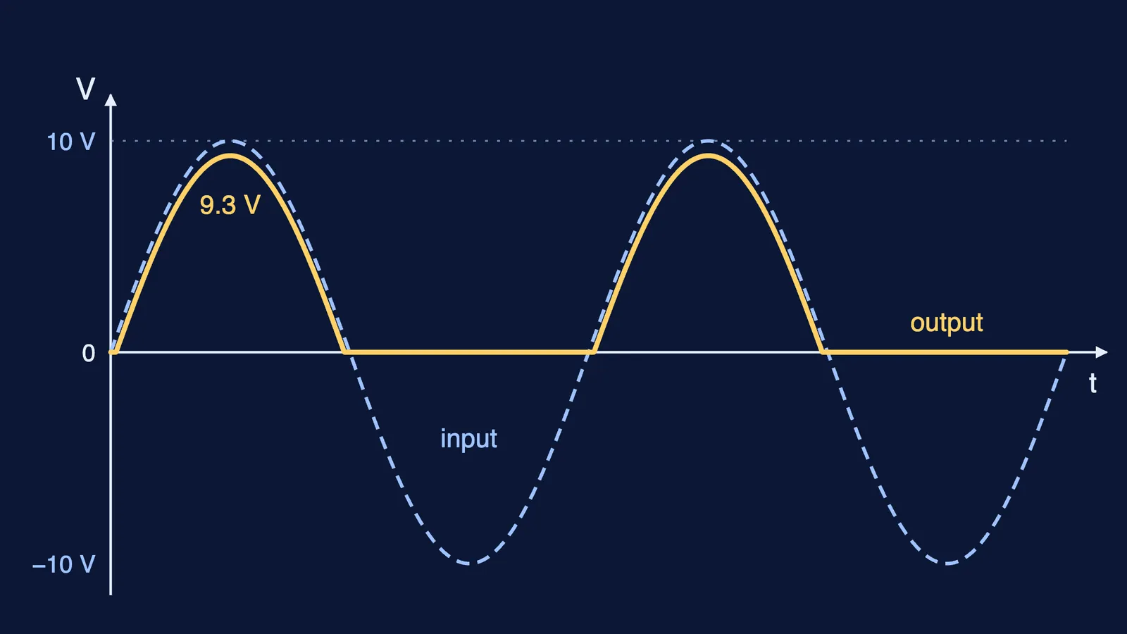
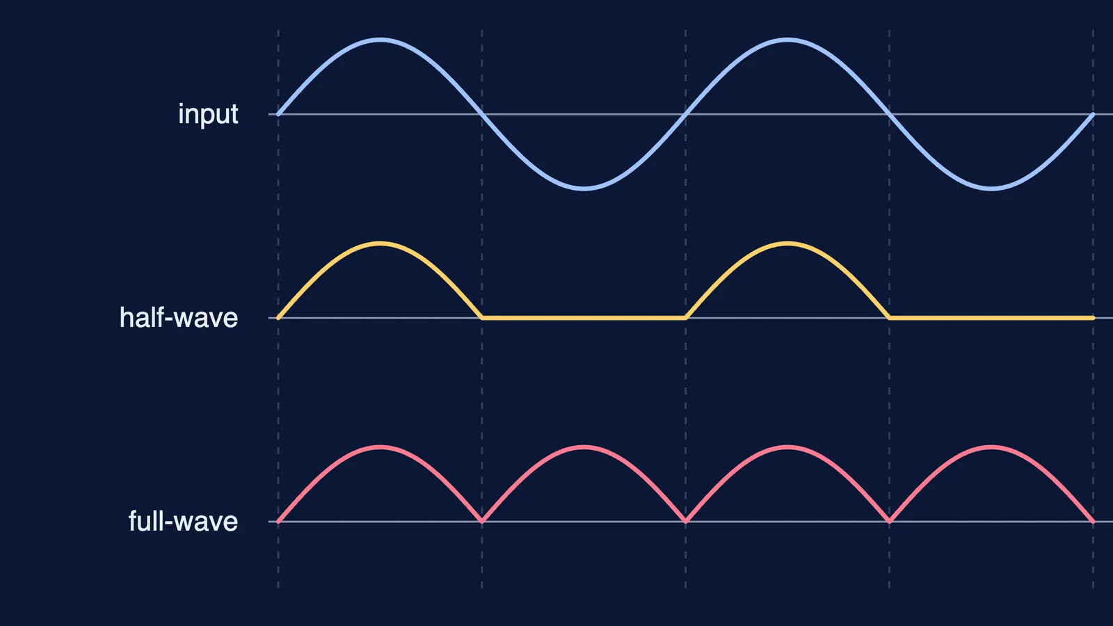
A half-wave rectifier passes only the half-cycles that forward-bias its diode, giving one pulse per input cycle; a full-wave rectifier uses both halves, giving two (NCERT). So a 200 Hz input gives a 200 Hz half-wave output and a 400 Hz full-wave output.
In the centre-tap circuit each diode works on one half of the secondary, NCERT points out, so with ideal diodes a 24 V peak secondary gives about 12 V peak.
How does a Zener diode regulate voltage?
Per the NIOS lesson, the Zener works in reverse bias, holding its breakdown voltage while a series resistor takes up the difference: Is = (Vi − Vz)/Rs, Iz = Is − IL, and the load must draw less than Is.
Worked example. A 9.0 V supply, a 100 Ω series resistor and a 5.0 V Zener.
Series current = (9.0 − 5.0)/100 = 40 mA.
With a 250 Ω load, IL = 20 mA, so Iz = 20 mA and the output holds at 5.0 V.
With a 100 Ω load, the load would need 50 mA, more than the 40 mA available. The Zener leaves breakdown; the output becomes a plain divider, 9.0 × 100/200 = 4.5 V.
Ignoring the Zener's minimum current, the smallest regulating load is 5.0 V / 40 mA = 125 Ω.
How do you solve combined logic gate questions?
Learn each gate as four outputs for AB = 00, 01, 10, 11, from the NIOS truth tables:
AND: 0, 0, 0, 1
OR: 0, 1, 1, 1
NAND: 1, 1, 1, 0
NOR: 1, 0, 0, 0
NOT: 0 gives 1, and 1 gives 0
Worked example. A passes through a NOT gate; NOT A and B feed a NOR gate, so Y = NOT (NOT A OR B). Row by row:
A = 0, B = 0: NOT A = 1, OR = 1, Y = 0
A = 0, B = 1: NOT A = 1, OR = 1, Y = 0
A = 1, B = 0: NOT A = 0, OR = 0, Y = 1
A = 1, B = 1: NOT A = 0, OR = 1, Y = 0
Y is 1 only when A = 1 and B = 0, so Y = A AND (NOT B). Inverting B instead gives (NOT A) AND B.
A one-week plan for this unit
Day 1: NCERT on doping and the junction; Exercises 14.1 to 14.5 without notes.
Day 2: Redo the two-diode example with germanium (0.2 V each).
Day 3: Sketch rectifier outputs; NCERT Exercise 14.6.
Day 4: Vary the Zener example's load until regulation fails.
Day 5: Build AND, OR and NOT from NAND gates only, then from NOR gates only.
Day 6: Our guide to the Zener diode reverse characteristic practical, a listed Experimental Skill.
Day 7: A timed mixed set; label each mistake by topic.
When an answer is wrong and you cannot see why, the Fermi Problem Library has worked problems with a step-by-step solver that explains the reasoning rather than printing an answer, so you can find the faulty line.