
On this page
Semiconductor Electronics has few formulas. The CBSE Class XII Physics curriculum for 2026-27 limits it to energy bands (qualitative ideas only), intrinsic and extrinsic semiconductors, the p-n junction, diode I-V characteristics and the diode as a rectifier. Every formula below comes from the NCERT Chapter 14 text, with symbols, SI units and the condition each one needs.
Not in the 2026-27 theory syllabus: transistors, Zener diodes, LEDs, photodiodes, solar cells and logic gates. LEDs appear only in the practical activities (identifying one and checking its one-way conduction with a multimeter), with no formula attached. NCERT gives no average-output or ripple formulas for rectifiers either. For the exam pattern, read our Semiconductor Electronics Class 12 board exam guide.
Energy bands and resistivity
ρ = 1/σ. ρ is resistivity (Ω m), σ is conductivity (S m⁻¹).
Typical ranges from NCERT: metals ρ ~ 10⁻² to 10⁻⁸ Ω m; semiconductors ρ ~ 10⁻⁵ to 10⁶ Ω m; insulators ρ ~ 10¹¹ to 10¹⁹ Ω m.
Eg = EC − EV. Eg is the band gap (eV), EC the bottom of the conduction band, EV the top of the valence band.
Classification: insulators Eg > 3 eV; semiconductors Eg < 3 eV (NCERT's summary gives 0.2 eV to 3 eV); metals Eg ≈ 0, or overlapping bands.
Values to remember: C (diamond) 5.4 eV, Si 1.1 eV, Ge 0.7 eV, Sn 0 eV.
Worked example: a sample has σ = 2.5 × 10⁻³ S m⁻¹. Then ρ = 1/(2.5 × 10⁻³) = 400 Ω m, which sits inside the semiconductor range.
Watch for: σ and ρ run in opposite directions.
What is the formula for electron and hole concentration?
Intrinsic semiconductor: ne = nh = ni. ne and nh are the numbers of free electrons and holes per unit volume (m⁻³); ni is the intrinsic carrier concentration.
Current in an intrinsic semiconductor: I = Ie + Ih, the electron and hole currents added.
n-type (pentavalent donors such as As, Sb, P): ne ≫ nh, and with doping much larger than ni, ne ≈ ND, the donor concentration.
p-type (trivalent acceptors such as B, Al, In): nh ≫ ne, and by the same reasoning nh ≈ NA, the acceptor concentration.
Mass action law: ne nh = ni². It holds in thermal equilibrium, for intrinsic and doped material.
Worked example: pure Si has 5 × 10²⁸ atoms m⁻³ and ni = 1.5 × 10¹⁶ m⁻³ (the values NCERT uses in Example 14.2). Dope it with boron at 2 ppm.
NA = 2 × 10⁻⁶ × 5 × 10²⁸ = 1 × 10²³ m⁻³, so nh ≈ 1 × 10²³ m⁻³.
ne = ni²/nh = (2.25 × 10³²)/(1 × 10²³) = 2.25 × 10⁹ m⁻³.
Watch for: doping does not raise both carriers. The majority carrier rises and the minority carrier falls, because their product stays fixed at ni². Also, 1 ppm is 10⁻⁶, not 10⁻³.
p-n junction and diode formulas
Barrier with no bias: V0, the barrier potential (V).
Forward bias (p-side to the positive terminal): effective barrier = V0 − V, where V is the applied voltage.
Reverse bias (n-side to the positive terminal): effective barrier = V0 + V.
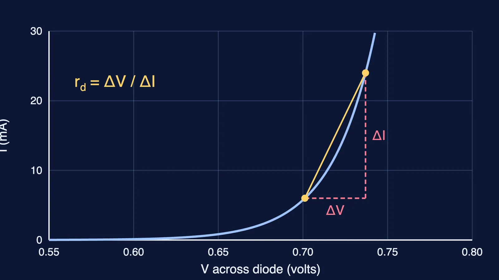
Cut-in (threshold) voltage: about 0.7 V for a silicon diode and about 0.2 V for a germanium diode.
Dynamic resistance: rd = ΔV/ΔI (Ω), for a small change ΔV in voltage and the matching small change ΔI in current.
In reverse bias the current is the small reverse saturation current, almost independent of voltage up to the breakdown voltage Vbr.
Worked example: on a silicon diode's curve, the current is 12 mA at 0.72 V and 24 mA at 0.78 V. Then rd = (0.78 − 0.72)/(0.024 − 0.012) = 0.06/0.012 = 5 Ω. With V0 = 0.7 V, a forward bias of 0.3 V leaves a barrier of 0.4 V, and a reverse bias of 5 V raises it to 5.7 V.
Watch for: convert mA to A before dividing. Forward currents are in mA; reverse currents are far smaller, in µA or less.
How do you find the output of a rectifier?
Output frequency of a half-wave rectifier = f, the input frequency (Hz). Output frequency of a full-wave rectifier = 2f. (This is NCERT Exercise 14.6: for 50 Hz input, 50 Hz and 100 Hz.)
Centre-tap full-wave rectifier: each diode rectifies half the total secondary voltage.
The diode's reverse breakdown voltage must be sufficiently higher than the peak ac voltage at the secondary.
Capacitor filter: time constant τ = C RL (s), with C in farads and RL in ohms. A larger τ keeps the output nearer the peak.
Worked example: a centre-tap transformer gives 24 V peak across the whole secondary at 50 Hz, with RL = 1 kΩ and C = 470 µF.
Each diode rectifies 12 V peak, half the secondary.
Output frequency is 2 × 50 = 100 Hz, so a new peak arrives every 10 ms.
τ = 470 × 10⁻⁶ × 1000 = 0.47 s, about 47 times the 10 ms gap, so the capacitor loses little charge between peaks.
Watch for: in a centre-tap circuit, using the full secondary peak as the output peak doubles your answer.
How to revise this formula sheet
Rewrite the five carrier relations (ne = nh = ni, I = Ie + Ih, ne ≈ ND, nh ≈ NA, ne nh = ni²) from memory, then redo the boron example with 5 ppm.
Learn the four band gap values together with the 3 eV dividing line.
Sketch an I-V curve with mA and µA scales and mark the 0.7 V knee; take rd from two points on it.
Answer NCERT Exercise 14.6 aloud, then repeat it for a 60 Hz supply.
If the barrier or the rectified waveform is hard to picture, the Fermi Simulation Lab has interactive simulations for the ideas that are easier to see than to read.
For JEE-style circuits on the same ideas, see Semiconductors for JEE Main: how to prepare, with worked circuits.