
On this page
Eight original JEE Main-style questions on semiconductors, easy to hard, each with a worked solution and a trap line for the most tempting wrong option. Q5 is numerical.
How should you use this semiconductor question set?
Unit 19 (Electronic Devices) of the NTA's Syllabus for JEE (Main) - 2027 lists semiconductors, diode I-V characteristics, the rectifier, the LED, photodiode, solar cell and Zener diode, the Zener regulator, and the OR, AND, NOT, NAND and NOR gates. The JEE (Main) 2027 information bulletin gives +4 for a correct answer and −1 for a wrong one, and Section B answers are rounded to the nearest integer.
Take 20 minutes, on paper, no calculator.
For every diode, decide first whether it is on or off, then write the equation.
Read every trap line, even where you were right.
New to the unit? Read our guide on how to prepare semiconductors for JEE Main. If one method keeps failing, the Fermi Problem Library has worked problems with a step-by-step solver that explains the reasoning rather than printing an answer.
Easy: can you handle carriers, bias and a single diode?
These three use the NCERT Semiconductor Electronics chapter: the law nₑnₕ = nᵢ², and the effective barrier (V0 − V) in forward bias and (V0 + V) in reverse bias.
Q1 (easy). Pure silicon at room temperature has nᵢ = 1.5 × 10¹⁶ m⁻³. It is doped with 3.0 × 10²¹ donor atoms per m³, all ionised. The hole density is:
(A) 1.5 × 10¹⁶ m⁻³
(B) 7.5 × 10¹⁰ m⁻³
(C) 7.5 × 10¹¹ m⁻³
(D) 3.0 × 10²¹ m⁻³
Answer: (B). nₑ ≈ donor density, so nₕ = nᵢ²/nₑ = (2.25 × 10³²)/(3.0 × 10²¹) = 7.5 × 10¹⁰ m⁻³. Trap: (A), which forgets that extra electrons suppress the holes.
Q2 (easy). A junction has a built-in barrier V0 = 0.70 V. Its p-side is held at −2.0 V and its n-side at +1.0 V. The effective barrier and the depletion region are:
(A) 2.3 V, wider
(B) 0.70 V, unchanged
(C) 3.7 V, narrower
(D) 3.7 V, wider
Answer: (D). The n-side is 3.0 V higher: reverse bias, so barrier = V0 + V = 3.7 V, and the depletion region widens. Trap: (A), which takes V − V0 instead of adding the bias to the barrier.
Q3 (easy). A 6.0 V cell, a 470 Ω resistor and a forward-biased silicon diode (take 0.7 V across it when on) are in series. The current is closest to:
(A) 11.3 mA
(B) 12.8 mA
(C) 14.3 mA
(D) zero
Answer: (A). I = (6.0 − 0.7)/470 = 11.3 mA. Trap: (B), which ignores the diode's drop.
Medium: where do Zener, LED and gate questions trip you up?
The Zener relations come from the NIOS lesson on semiconductor devices: Is = (Vi − Vz)/Rs and Iz = Is − IL, with the Zener in reverse bias.
Q4 (medium). A 15 V supply feeds a 6.2 V Zener through a 220 Ω series resistor, with a 1.0 kΩ load across the Zener. The Zener current is:
(A) 40.0 mA
(B) 46.2 mA
(C) 33.8 mA
(D) 25.0 mA
Answer: (C). Without the Zener the load would see 12.3 V, so it breaks down. Is = 8.8/220 = 40.0 mA, IL = 6.2/1000 = 6.2 mA, so Iz = 33.8 mA. Trap: (A), which forgets the load takes its share.
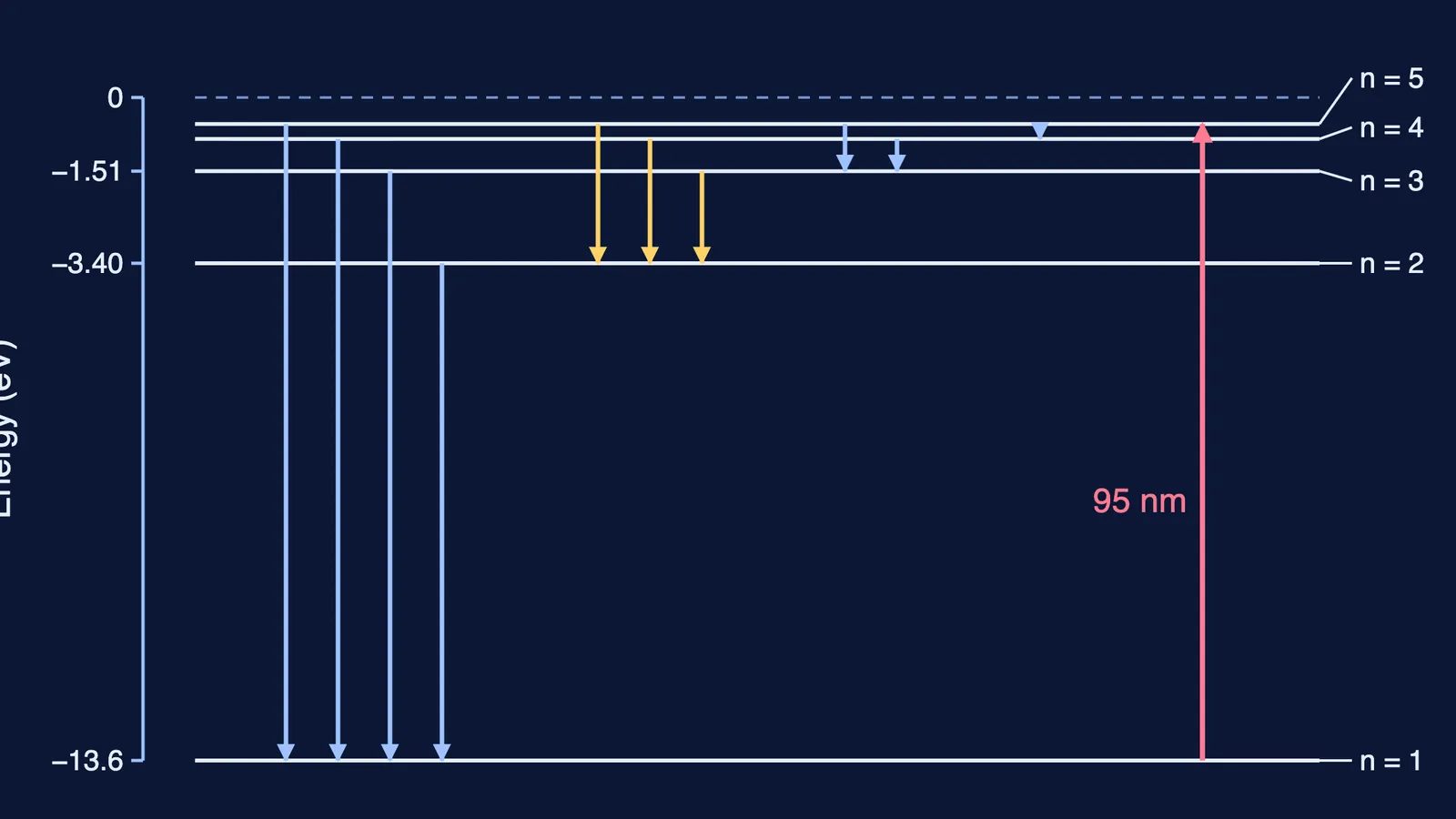
Q5 (medium, numerical). An LED's semiconductor has a band gap of 1.9 eV, and each emitted photon carries that energy. Using hc = 1240 eV nm, find the wavelength in nm.
Answer: 653. λ = 1240/1.9 = 652.6 nm (red), so enter 653. Trap: entering 1, from working in micrometres (0.65 μm) in an integer-answer box.
Q6 (medium). A and B feed an OR gate. A and the OR output then feed a NAND gate, whose output is Y. Y equals:
(A) A NAND B
(B) NOT A
(C) NOT B
(D) A NOR B
Answer: (B). Y = NOT[A·(A + B)], and A·(A + B) = A, so Y = NOT A. For AB = 00, 01, 10, 11, Y = 1, 1, 0, 0. Trap: (A), which differs only at A = 1, B = 0, where the NAND sees 1 and 1.
Hard: can you spot when a Zener stops regulating or a diode stays off?
Q7 uses the rule that a minimum Zener current must always flow, typically 5 mA to 20 mA per the NIOS lesson.
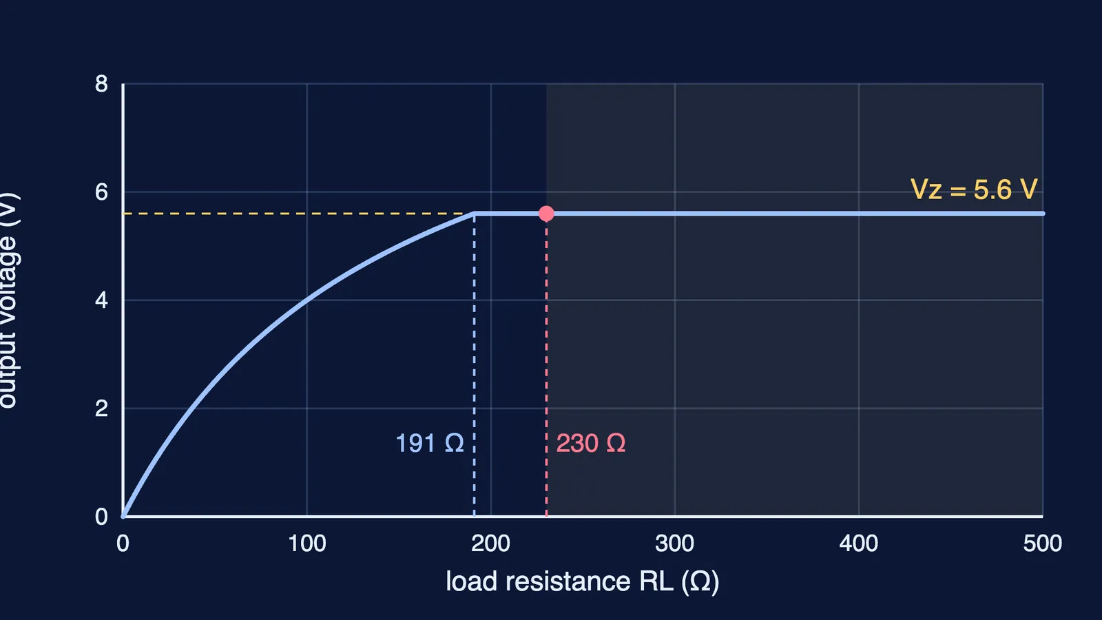
Q7 (hard). A 10.0 V supply, a 150 Ω series resistor and a 5.6 V Zener that needs at least 5.0 mA to stay in breakdown. The smallest load resistance that keeps the output at 5.6 V is closest to:
(A) 150 Ω
(B) 191 Ω
(C) 411 Ω
(D) 230 Ω
Answer: (D). Is = (10.0 − 5.6)/150 = 29.3 mA. The load may take at most 29.3 − 5.0 = 24.3 mA, so RL = 5.6/0.0243 ≈ 230 Ω. Trap: (B), which lets the Zener current fall to zero.
Q8 (hard). A 6.0 V cell and a 500 Ω resistor feed point X. From X to the cell's negative terminal, two forward-biased branches sit in parallel: a silicon diode (0.7 V when on) and two germanium diodes in series (0.3 V each). Treat each diode as a fixed drop once on. Find the silicon diode's current, then its current after a third germanium diode joins the string.
(A) 0 and 10.6 mA
(B) 5.4 mA and 10.6 mA
(C) 0 and 10.2 mA
(D) 10.8 mA and 0
Answer: (A). Two germanium diodes turn on at 0.6 V, below silicon's 0.7 V, so silicon stays off and the string carries (6.0 − 0.6)/500 = 10.8 mA. Three need 0.9 V, so silicon conducts first: (6.0 − 0.7)/500 = 10.6 mA. Trap: (B), which splits the current as if the branches were equal resistors.
What should you do with your score?
Sort wrong answers by type: bias (Q1-Q2), diode on or off (Q3, Q8), Zener (Q4, Q7), LED and gates (Q5-Q6). Our post on common mistakes in semiconductor questions goes through the usual causes, and ideal diode circuit problems gives more on-or-off practice. Redo the set in a week, solutions covered.