
On this page
Semiconductor Electronics is Chapter 14 of the NCERT Class 12 Physics textbook, Part 2. The CBSE Physics curriculum for 2026-27 limits it to energy bands (qualitative only), semiconductors, the p-n junction, diode characteristics and rectifiers. Transistors, Zener diodes, LEDs, photodiodes, solar cells and logic gates are in neither, so they are left out. For answers and traps, see our Semiconductor electronics Class 12 board exam guide.
How are metals, semiconductors and insulators told apart?
Resistivity classification: sorting solids by how strongly they resist current. Si and Ge are elemental semiconductors; GaAs and CdS are compounds. In the NCERT chapter, metals sit near 10^-2 to 10^-8 Ω m, semiconductors near 10^-5 to 10^6 Ω m and insulators near 10^11 to 10^19 Ω m.
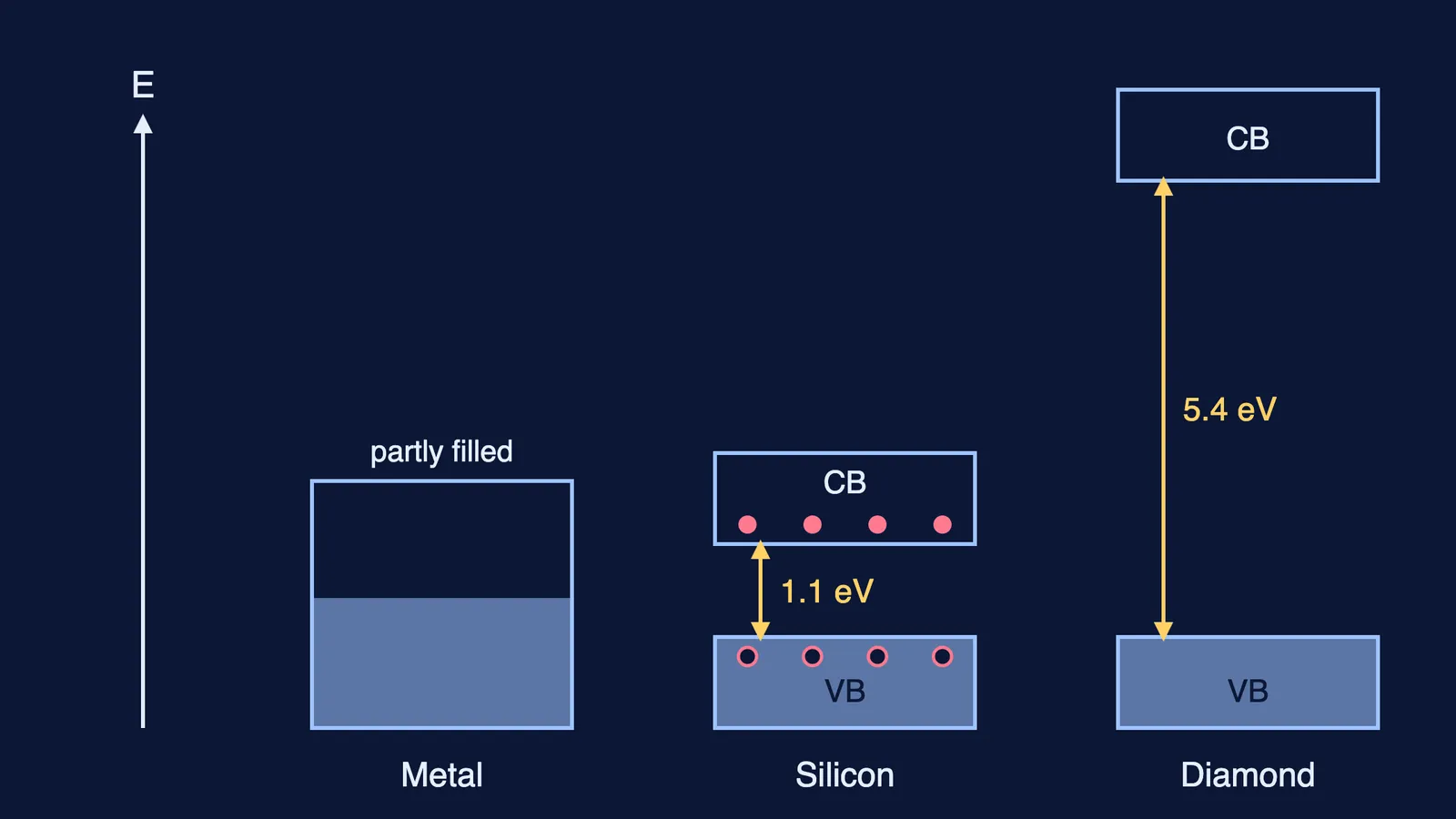
Energy band: a near-continuous range of electron energy levels formed when atoms pack into a crystal.
Valence band: the band holding the valence electrons; full in Si or Ge at 0 K.
Conduction band: the next band up; electrons there are free to carry current. It is empty in a pure semiconductor at 0 K.
Energy band gap (Eg): EC − EV, how far the conduction band's lowest level sits above the valence band's highest. Example: diamond 5.4 eV, Si 1.1 eV, Ge 0.7 eV, tin 0 eV.
Metal (band picture): a partly filled conduction band, or one overlapping the valence band.
Insulator and semiconductor (band picture): NCERT takes a gap above 3 eV as an insulator and a gap below 3 eV as a semiconductor. Don't confuse with: crystal structure. Diamond, Si and Ge share one lattice type; the gap separates them.
What is the difference between intrinsic and extrinsic semiconductors?
Intrinsic semiconductor: a pure semiconductor (each atom covalently bonded to four neighbours) whose carriers come only from heat breaking bonds, so free electrons equal holes: ne = nh = ni. At 0 K it acts as an insulator.
Hole: the empty spot left in a bond when an electron breaks free; it behaves like a carrier with charge +q. Total current is electron plus hole current, I = Ie + Ih. Don't confuse with: a real positive particle. A hole "moves" because neighbouring bound electrons hop into the vacancy.
Intrinsic carrier concentration (ni): electrons (or holes) per unit volume in a pure sample. Example: NCERT uses ni = 1.5 × 10^16 m^-3 for Si.
Doping and extrinsic semiconductor: deliberately adding a few parts per million of a chosen impurity (the dopant), with atoms about the host's size; the doped, far more conductive result is extrinsic.
Donor and n-type: a pentavalent dopant (As, Sb, P) gives a spare, loosely held electron, making electrons the majority carriers and holes the minority (ne >> nh). Example: freeing that electron takes about 0.05 eV in Si.
Acceptor and p-type: a trivalent dopant (B, Al, In) leaves one bond short of an electron, making holes the majority carriers (nh >> ne).
Donor and acceptor levels: dopant energy levels, ED just below EC and EA just above EV.
Mass-action relation: ne × nh = ni^2 in equilibrium. Example: NCERT's 1 ppm arsenic in Si gives about 5 × 10^22 electrons but only about 4.5 × 10^9 holes per m^3.
Charge neutrality: a doped crystal stays neutral; ionised dopant cores balance the extra carriers. Don't confuse with: "n-type is negatively charged". It is not.
What happens at a p-n junction?
p-n junction: the boundary made inside one crystal when part of a p-type wafer is doped to n-type. Don't confuse with: pressing two slabs together, which cannot give atom-level contact.
Diffusion and diffusion current: carriers spreading from high to low concentration, holes p to n and electrons n to p.
Depletion region (space-charge region): a layer about a tenth of a micrometre (NCERT), with no free carriers, only fixed ions: positive donors on the n-side, negative acceptors on the p-side.
Drift and drift current: carriers pushed by the junction's field, opposite to diffusion. At equilibrium they balance: zero net current.
Barrier potential (V0): the built-in voltage across the junction, n-side positive, that stops further diffusion.
How does a junction diode behave in forward and reverse bias?
Semiconductor diode: a p-n junction with metal contacts, a two-terminal device. Its symbol's arrow points along conventional current in forward bias.
Forward bias: p-side to positive. The barrier drops to V0 − V, the depletion layer narrows and current reaches milliamperes.
Minority carrier injection: in forward bias, electrons enter the p-side and holes the n-side as minority carriers.
Reverse bias: n-side to positive. The barrier rises to V0 + V and the depletion layer widens.
Threshold (cut-in) voltage: the forward voltage after which current climbs sharply. Example: about 0.7 V for Si, 0.2 V for Ge (NCERT).
Reverse saturation current: the tiny, nearly constant reverse current, set by minority-carrier numbers, not voltage.
Breakdown voltage (Vbr): the reverse voltage where current suddenly shoots up. Don't confuse with: cut-in voltage, which is in forward bias.
Dynamic resistance (rd): ΔV/ΔI from the I-V curve. Example: NCERT's 0.1 V change for a 10 mA change gives 10 Ω.
How does a diode turn AC into DC?
Rectifier (NCERT): a circuit using a diode's one-way conduction to turn AC into one-way voltage.
Half-wave rectifier: one diode; output only in the half-cycles when it is forward biased. Example: a 50 Hz input gives a 50 Hz output.
Full-wave rectifier: two diodes on a centre-tap transformer, each conducting in alternate half-cycles, so both halves appear at the output. Example: a 50 Hz input gives 100 Hz.
Filter: rectified output flows one way but in half-sine pulses; a capacitor across the load, or an inductor in series, smooths it towards steady DC. A larger time constant, C × RL, smooths it more.
How to learn these terms
Learn them in pairs: donor/acceptor, diffusion/drift, forward/reverse bias, cut-in/breakdown.
Draw the three band pictures from memory, then the junction with its fixed ions.
For each bias, note barrier height, depletion width and current size.
Sketch half-wave and full-wave outputs under the input sine wave.
If drift and diffusion are hard to picture, the Fermi Simulation Lab has interactive simulations for ideas that are easier to see than to read. For worked diode circuits, try our ideal diode circuit problems.