
On this page
India is now building the factories that make chips, not just the phones that use them. In February 2024 the Union Cabinet approved a semiconductor fab by Tata Electronics with Taiwan's PSMC at Dholera, Gujarat, at an estimated cost of Rs 91,000 crore, as ThePrint reported. Tata Electronics says the planned plant is a 300 mm fab expected to have a capacity of 50,000 wafers a month, making analog and logic chips at 28 nm to 110 nm. The India Semiconductor Mission's fab scheme gives approved projects fiscal support of 50% of the project cost.
What is a silicon wafer?
A wafer is a thin, polished disc of silicon on which many chips are built at once. ASML, which makes lithography machines, says wafers are sliced from a salami-shaped bar, or ingot, of 99.99% pure silicon and polished to extreme smoothness. The same page says 300 mm is the wafer size most often used, and that finished wafers are cut with a diamond saw into individual chips called dies.
How are semiconductor chips made, step by step?
Modern chips can have up to 100 layers, all aligned to nanometre precision, according to ASML's guide to how microchips are made. Each layer goes through roughly the same loop, described in ASML's six steps of chip manufacturing:
Deposition: a thin film of conducting, insulating or semiconducting material is laid on the wafer.
Photoresist coating: the wafer is covered with a light-sensitive coating called photoresist.
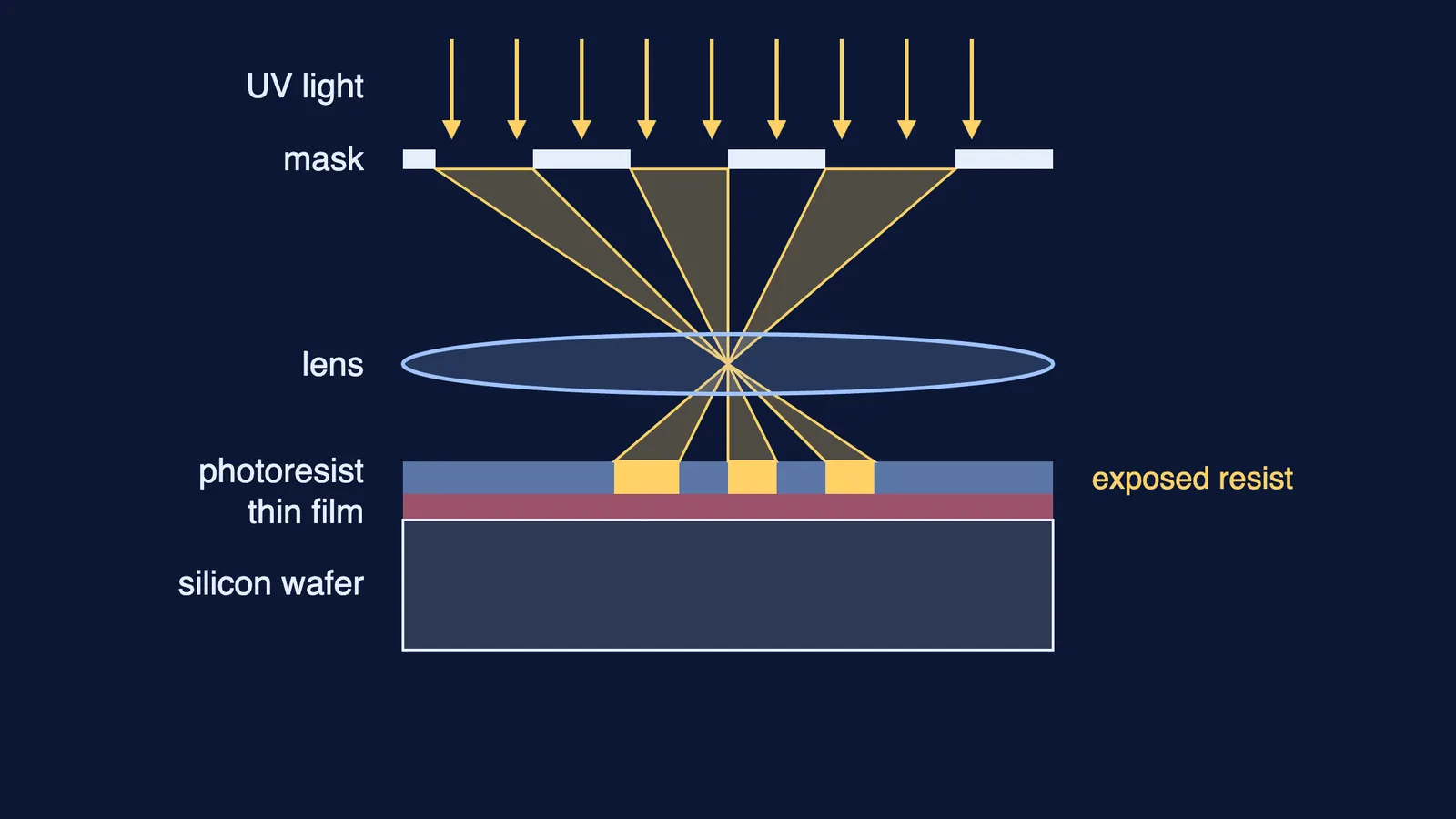
Lithography: light shines through a mask carrying the circuit pattern, and optics shrink and focus it onto the wafer.
Etching: the resist is developed, some is washed away, and the open areas are etched into a 3D pattern.
Ion implantation: charged ions are fired into the silicon to control how it conducts, which is how transistors are made.
Repeat, then package: after the last layer, the wafer is diced into chips.
What is photolithography, and why does wavelength matter?
Photolithography is printing with light: a pattern on a mask, or reticle, is projected through optics onto a light-sensitive silicon wafer, as ASML explains. ASML's deep ultraviolet (DUV) machines use laser light at 248 nm and 193 nm, and its extreme ultraviolet (EUV) machines use 13.5 nm light, more than 14 times shorter than DUV (ASML on light and lasers).
If a lens shrinking a pattern onto a wafer is hard to picture, the Fermi Simulation Lab has interactive simulations for ideas that are easier to see than read.
What does doping do to silicon?
Doping means adding a small percentage of foreign atoms to the silicon crystal, which changes its electrical properties dramatically (HyperPhysics, Georgia State University). Pentavalent atoms such as phosphorus or arsenic add free electrons and make n-type silicon. Trivalent atoms such as boron or gallium create holes and make p-type silicon.
In a fab, the pattern left by lithography and etching decides which parts of the wafer the ions reach, so the p and n regions sit where the design says. Where they meet you get the p-n junction from your NCERT chapter. Our explainer on why a voltmeter can't measure a p-n junction's barrier potential picks up from there, and the idea of the transistor itself goes back to Lilienfeld's 1925 field-effect transistor patent.
If n-type and p-type feel abstract, the Fermi Concept Library covers every concept in physics, chemistry, biology, mathematics and computing.
Why do chip fabs need clean rooms?
Even the smallest speck of dust landing on a wafer can ruin a chip, so chip clean rooms are about 10,000 times cleaner than outside air, according to ASML. Most chipmakers use "ISO class 1" rooms with no more than 10 particles of 100 to 200 nm per cubic metre of air; a clean, modern hospital has about 10,000 dust particles per cubic metre, ASML says.
Worked example: how many chips fit on one wafer?
The Dholera plant is a planned 300 mm fab with a capacity of 50,000 wafers a month (Tata Electronics).
Wafer radius is 150 mm, so its area is π × 150² ≈ 70,700 square mm.
Suppose each die is 10 mm × 10 mm, or 100 square mm.
Upper limit: 70,700 ÷ 100 ≈ 707 dies per wafer.
The real number is lower: square dies cannot fill the curved edge, and dust or a misaligned layer spoils some dies.
At 50,000 wafers a month, that upper limit is about 35 million dies a month.
Halve the die to 5 mm × 5 mm and the count roughly quadruples. Smaller dies mean more chips from every wafer.
If you get stuck on an estimate like this, the Fermi Problem Library has a step-by-step solver that explains the reasoning.
Next, read our guide to the difference between a CPU and a GPU, and why AI trains on GPUs.