
On this page
Your phone and laptop run on field-effect transistors. The basic idea behind them was patented by a physicist who left Leipzig for the United States. That was Julius Edgar Lilienfeld. He filed in Canada in October 1925 and in the US in 1926, more than thirty years before anyone made the device work.
Born in Lemberg (now Lviv) in 1882, he earned his doctorate in Berlin and moved to the United States in 1921 to pursue his patent claims, according to his Wikipedia biography.
What did Lilienfeld's 1925 patent describe?
The patent is US 1,745,175, "Method and apparatus for controlling electric currents". It was filed in the US on 8 October 1926, claims a Canadian priority date of 22 October 1925 and was granted in January 1930, as the Google Patents record shows. It offered a solid-state replacement for the vacuum tube, with no hot filament and no evacuated space.
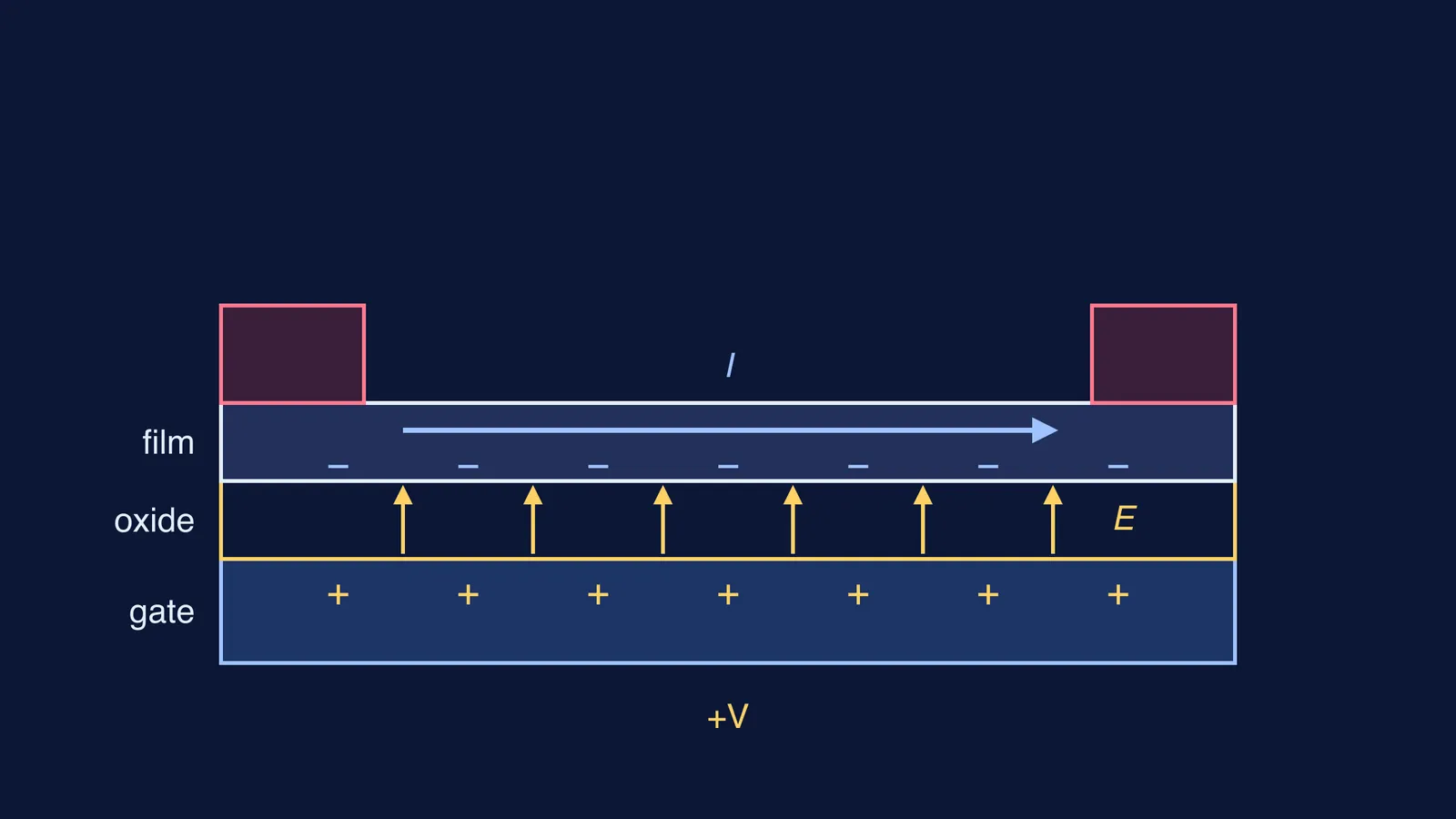
A glass block was fractured and a strip of aluminium foil about one ten-thousandth of an inch thick was held in the break. Metal coatings on either side served as terminals, and a thin film of a copper-sulphur compound was laid over them. A voltage on the foil was meant to control the current through the film.
His later patent, US 1,900,018, was filed in March 1928 and granted in March 1933. In it, an aluminium base carries an insulating layer of aluminium oxide of "minute thickness", with a more conductive coating on top, according to its patent text. The aim was to subject a conducting layer of "extreme thinness (approaching molecular thickness)" to a very strong electrostatic field. That metal-insulator-conductor stack is the shape of today's MOS transistor.
Did Lilienfeld ever build a working transistor?
As far as anyone can prove, no. The Computer History Museum says "no records exist to prove that Heil or Lilienfeld actually constructed functioning devices". Oskar Heil filed a similar patent in 1934.
The patents still mattered. In 1948 Bell Labs filed patent applications on its early work exploring William Shockley's field-effect idea. The US Patent Office said they were "too similar to the Lilienfeld work done almost 20 years before", PBS reports. Those were rejected; the patents granted covered the point-contact and junction transistors.
Why did the field-effect transistor take until 1959 to work?
The trouble was at the surface. According to the Computer History Museum, John Bardeen calculated in 1946 that surface effects could explain why attempts to build these devices had failed. Charge trapped in surface states screens the gate's field from the electrons that carry the current.
The fix came from John Atalla and Dawon Kahng at Bell Labs. They found that surface states could be markedly reduced where silicon meets a layer of thermally grown silicon dioxide. In 1959 they achieved the first successful insulated-gate field-effect transistor, demonstrated in 1960, the Computer History Museum records. The same page says over 99 percent of microchips produced today use MOS transistors.
Can a gate voltage really move enough electrons? A worked example
You can check Lilienfeld's idea with a Class 12 capacitor formula. Treat the gate and the film as the two plates of a parallel-plate capacitor, with a thin aluminium oxide layer in between.
Pick an illustrative oxide thickness, not Lilienfeld's figure: d = 10 nm = 1 × 10⁻⁸ m.
Take a relative permittivity of about 9 for aluminium oxide. One RIT study measured 8.83 ± 0.55 and cites a literature value of 9.0.
Capacitance per area: C/A = ε₀εᵣ/d = (8.85 × 10⁻¹² × 9) / 10⁻⁸ ≈ 8.0 × 10⁻³ F/m².
At 1 V the gate induces a charge of about 8.0 × 10⁻³ C/m². Divide by e (1.6 × 10⁻¹⁹ C) and you get about 5 × 10¹⁶ extra electrons per square metre.
Now compare that with a metal. Copper has 8.47 × 10²⁸ free electrons per cubic metre, according to HyperPhysics. A layer just 1 nm thick already holds about 8.5 × 10¹⁹ per square metre.
So the gate shifts only about 0.06% of the electrons in one nanometre of copper; a metal film barely notices. A semiconductor film 100 nm thick with an illustrative 10²² carriers per cubic metre holds only 10¹⁵ per square metre, so the same gate charge is about 50 times what is already there. That is why the idea needs a semiconductor and a thin film, and why trapped surface charge could cancel it.
What can you take from Lilienfeld as a student?
Separate the principle from the build: ask what physics an invention relies on and what material it was waiting for.
Put numbers on a claim. Five lines of capacitor maths told you more than a paragraph of description.
Read primary sources. Patents are free to read on Google Patents.
The Fermi Simulation Lab has interactive simulations for ideas that are easier to see than to read. To revise capacitance and permittivity first, open the Fermi Concept Library.
Next, redo the worked example at 5 V and see how the electron count scales.