
On this page
If you have a smartphone in your pocket, you are carrying a piece of interplanetary technology. Before the early 1990s, taking a high-quality digital photograph required a bulky, power-hungry device that was difficult to miniaturise. Today, tiny lenses are everywhere—from the backs of our phones to the bumpers of our cars. The difference is the Complementary Metal Oxide Semiconductor (CMOS) active pixel sensor, an invention by Dr. Eric Fossum that changed the trajectory of digital imaging.
Why did NASA need a new type of camera?
In the late 1980s, the standard for digital imaging was the Charge-Coupled Device (CCD). CCDs captured excellent images, but they shuttled electrical charges across the entire chip like a bucket brigade to a single output amplifier.
This process required multiple support chips and a significant amount of energy. When NASA needed to send spacecraft on long, interplanetary missions, weight and power were strictly limited. Fossum and his team at NASA’s Jet Propulsion Laboratory (JPL) were tasked with creating a "camera on a chip" that could survive deep space without draining the battery.
What is a CMOS active pixel sensor?
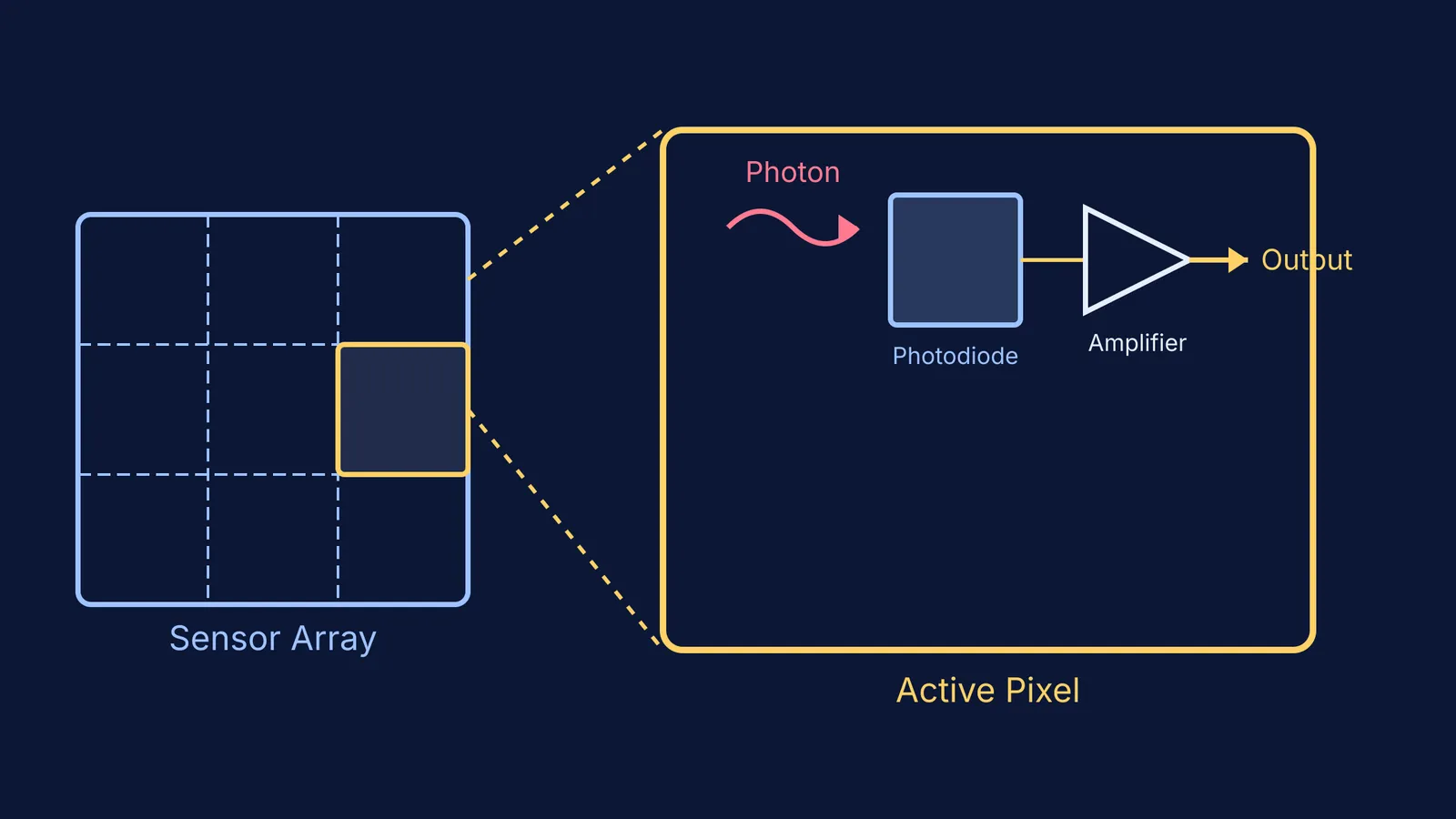
Between 1992 and 1993, Fossum's team solved the problem by rethinking how the chip handled light. Instead of moving all the charge to one corner, they placed an active amplifier inside every single pixel.
This "active pixel" design meant the sensor could convert the charge to a voltage directly on site. The CMOS sensor uses about 1% of the power required by older CCD systems (NASA Spinoff). By integrating the amplifier and noise reduction onto one piece of silicon, the technology reduced camera size by over 90% (NASA Spinoff).
If you are trying to understand how light is converted into an electrical signal—much like the photoelectric effect—the Fermi Concept Library has a lesson on the physics of semiconductors and photons. You can also explore related electronics concepts, such as how a microphone turns sound waves into electric current or how depletion layer width changes in forward and reverse bias.
How did the CMOS sensor change the world?
Realising the potential of the technology on Earth, Fossum co-founded Photobit in 1995 to commercialise the CMOS sensor (Wikipedia). Because the sensors could be manufactured using the same standard silicon processes used to build computer processors, they were cheap to mass-produce.
This manufacturing advantage led to many new applications. CMOS sensors made tiny computer webcams, robust automotive backup cameras, and swallowable "pill cameras" for noninvasive medical endoscopy a reality. The most significant impact, however, was the mobile phone. The low power draw and small physical footprint of the CMOS sensor made it an ideal fit for battery-powered smartphones. This single invention is responsible for putting a high-quality camera into the hands of people around the world, changing how we document and share our lives. Today, Dr. Fossum is a professor at Dartmouth College and continues to research next-generation imaging, such as sensors that can count individual photons (Wikipedia).
How to spot an engineering bottleneck: The "Camera on a Chip" checklist
Fossum's work is an example of identifying a bottleneck and redesigning the system to remove it. If you are working on a physics or engineering project, use this checklist to decide if your current design needs a fundamental rethink rather than a small tweak:
Power budget: Is one component consuming more than 50% of the available energy? (The CCD was draining spacecraft batteries).
Support structures: Does the core component require too many extra parts just to function? (CCDs needed external chips for timing and analog-to-digital conversion).
Scaling limits: Has the technology reached a physical limit where it can no longer be made smaller?
Harsh environments: Will the current materials degrade under extreme conditions? (CCDs were sensitive to cosmic radiation).
When you hit two or more of these limits, you cannot just optimise the old technology. Like moving the amplifier directly into the pixel, you have to change the architecture. (You might also find inspiration in everyday interfaces, like how a phone touchscreen senses your finger).