
On this page
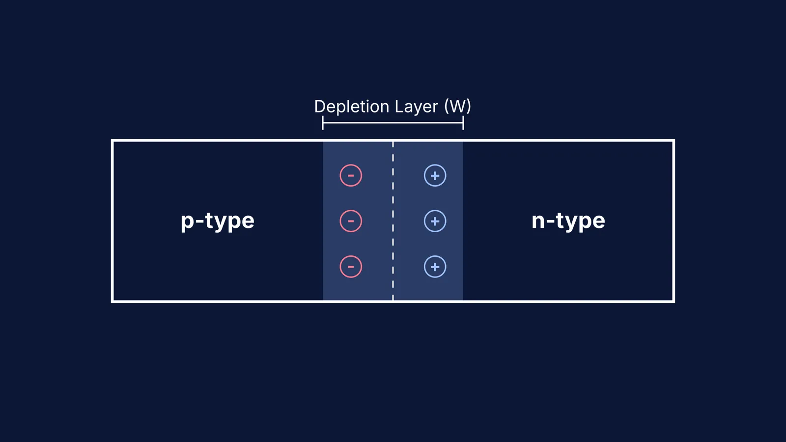
When a p-type and an n-type semiconductor meet, they form a p-n junction. At the boundary, electrons from the n-side diffuse across to fill holes on the p-side. This recombination leaves behind immobile charged ions—positive donors on the n-side and negative acceptors on the p-side. This area, stripped of mobile charge carriers, is called the depletion layer. It creates a built-in electric field that acts as a barrier, preventing further current from flowing under equilibrium conditions.
But the depletion layer is not fixed. Its width changes dramatically when you apply an external voltage, a process known as biasing. This adjustable width is the foundational mechanism that allows diodes to act as one-way valves and transistors to act as switches.
How do you calculate the width of the depletion layer?
The width (W) of an abrupt p-n junction depends on the semiconductor's material properties, the doping concentrations (N_a on the p-side and N_d on the n-side), and the total electrical potential across the junction. Without any external battery connected, this potential is exactly equal to the built-in potential (V_bi), which is typically 0.6 to 0.7 V for standard silicon junctions at room temperature.
The governing equation for the depletion width is:
W = √((2ε_s / q) × (1/N_a + 1/N_d) × (V_bi - V))
Here, ε_s is the permittivity of the semiconductor, q is the elementary charge (1.602 × 10⁻¹⁹ C), and V is the applied voltage. The most important takeaway for exams like JEE and NEET is the proportionality: the width scales with the square root of the net potential barrier (√(V_bi - V)).
If you are studying for your boards or entrance exams and are unsure about how doping levels interact with these variables, the Fermi Concept Library contains every concept in physics, chemistry, biology, mathematics and computing, each with its own lesson. Fermi's AI tutor holds a line of reasoning across the session until you see how carrier concentrations shape the barrier.
How does the depletion layer change in forward bias?
In forward bias, you connect the positive terminal of your external battery to the p-side and the negative terminal to the n-side.
This applied voltage (V) opposes the built-in potential (V_bi). If you look at the width equation, the term (V_bi - V) decreases because V is a positive number. Physically, the external electric field is pushing majority carriers—holes from the p-side and electrons from the n-side—directly toward the junction. As these mobile carriers flood into the depletion region, they neutralize some of the immobile ions at the edges.
As a result, the depletion layer shrinks. The potential barrier drops significantly, and once the applied voltage approaches the built-in potential, the barrier practically vanishes. This allows a large diffusion current to flow across the junction with very little resistance. For more on how carriers dictate electrical behavior, you can read our guide to n-type and p-type semiconductors.
How does the depletion layer change in reverse bias?
In reverse bias, you flip the battery connections: the positive terminal connects to the n-side and the negative terminal to the p-side.
Now, the applied voltage acts in the exact same direction as the built-in potential. In our formula, a reverse voltage is treated as negative (V < 0), meaning the voltage term becomes (V_bi - (-V)), or (V_bi + |V|). The total potential across the junction effectively increases.
Physically, the battery is pulling the majority carriers away from the junction. Holes are drawn toward the negative terminal, and electrons are drawn toward the positive terminal. This mass exodus exposes even more immobile ions on both sides, which widens the space charge region. The depletion layer grows, creating a massive barrier that blocks majority carriers entirely, leaving only a tiny leakage current generated by minority carriers. (To picture how these energy barriers prevent conduction, see our post on energy bands in semiconductors and insulators).
A framework for exam problems
When you face a numerical problem asking how much the width changes under different biases, you rarely need to plug in the permittivity of silicon or the elementary charge. Instead, rely on the ratio method.
Because W ∝ √(V_bi - V), you can compare two states (like equilibrium and a specific bias) using this simplified relationship:
W₂ / W₁ = √((V_bi - V₂) / (V_bi - V₁))
Worked Example: A silicon p-n junction has a built-in potential of 0.8 V. What happens to the depletion width if a reverse bias of 1.7 V is applied?
Identify the initial equilibrium state: V₁ = 0 V.
Identify the final reverse bias state: V₂ = -1.7 V (remember that reverse bias voltage is negative).
Set up the ratio:
W₂ / W₁ = √((0.8 - (-1.7)) / (0.8 - 0)) = √(2.5 / 0.8) = √(3.125) ≈ 1.77
The depletion width increases by a factor of 1.77. If you ever get stuck setting up these ratios during a practice test, you can bring the problem to the Fermi Problem Library. The step-by-step solver explains the reasoning rather than printing an answer, noticing where you are stuck and deciding whether to explain, ask, or show.