
On this page
You need one fact before any wiring: a NAND gate gives 0 only when both inputs are 1, and 1 in every other case. It is AND followed by NOT, which is where the name comes from. The NAND logic reference on Wikipedia sets out the standard constructions we check below.
NAND truth table (A, B → output):
0, 0 → 1
0, 1 → 1
1, 0 → 1
1, 1 → 0
Why is NAND called a universal gate?
A gate is universal when any logic circuit can be built from copies of that one gate alone. The argument has two steps.
Any truth table can be written with NOT, AND and OR only. For each row where the output is 1, write an AND term that is true only on that row (for the row A = 1, B = 0, that term is A AND NOT B), then OR all those terms together.
NOT, AND and OR can each be built from NAND gates, as the next three sections show.
Put the two steps together and NAND can build anything. Logicians call this property functional completeness.
The Internet Encyclopedia of Philosophy explains that every connective of propositional logic (apart from the constants) can be defined using only the Sheffer stroke, or only NOR, and notes that Charles Sanders Peirce had found the idea in a fragment dating from 1880. Henry Sheffer published his result in 1913 in Transactions of the American Mathematical Society. The same encyclopedia points out a twist: Sheffer's own operation was 'neither-nor', which is NOR, and the name 'Sheffer stroke' was attached to NAND later.
How do you make a NOT gate using only NAND?
Join both inputs of one NAND gate and feed A into them, so the output is A NAND A, as in the standard NAND constructions.
Check each row:
A = 0: the gate sees 0, 0, so the output is 1.
A = 1: the gate sees 1, 1, so the output is 0.
The output is always the opposite of A.
How do you make an AND gate using only NAND?
NAND is AND followed by NOT, so undo the NOT. The standard construction uses 2 gates: the first computes X = A NAND B, and the second is a NOT built from NAND, giving Y = X NAND X.
Check each row (A, B → X → Y):
0, 0 → X = 1 → Y = 0
0, 1 → X = 1 → Y = 0
1, 0 → X = 1 → Y = 0
1, 1 → X = 0 → Y = 1
Y is 1 only when both inputs are 1. That is AND.
How do you make an OR gate using only NAND?
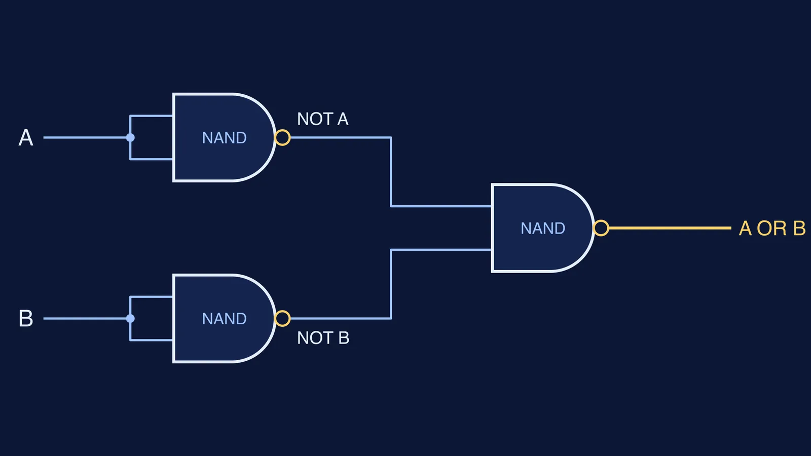
The standard construction uses 3 gates. Turn A into NOT A with one NAND (inputs tied), B into NOT B with a second, then feed both into a third: Y = (NOT A) NAND (NOT B), as in the diagram at the top.
Check each row (A, B → NOT A, NOT B → Y):
0, 0 → 1, 1 → Y = 0
0, 1 → 1, 0 → Y = 1
1, 0 → 0, 1 → Y = 1
1, 1 → 0, 0 → Y = 1
Y is 0 only when both inputs are 0. That is OR.
Why it works: P NAND Q means NOT (P AND Q), and De Morgan's law says NOT (P AND Q) = (NOT P) OR (NOT Q). Put P = NOT A and Q = NOT B, the double NOTs cancel, and you are left with A OR B. Our post on verifying De Morgan's laws with a Venn diagram shows the same law for sets.
How do you check a NAND-only circuit in an exam?
Use this routine on any NAND-only question:
Label every wire between gates with a letter (X, Y, P, Q).
Write the four input rows: 00, 01, 10, 11.
Fill the columns left to right, one gate at a time, using only the NAND rule: output 0 only if both inputs are 1.
Compare the last column with the target gate's truth table. If even one row differs, the wiring is wrong.
For circuits with several gates chained together, our guide to finding the output of any logic gate combination uses the same column method, and Boolean logic for CBSE Class 11 covers the full gate set with De Morgan's laws.
If a gate question goes wrong and you cannot see which row broke, the Fermi Problem Library has worked problems with a step-by-step solver that explains the reasoning rather than printing an answer. If the gap is the idea itself, the Fermi Concept Library has a lesson for every concept in physics, chemistry, biology, mathematics and computing.
Next step: build NOR from NAND gates with the same four-row check.