
On this page
You have probably memorised that Zener diodes are heavily doped. The reason sits in one formula: more doping gives a thinner depletion layer, a stronger field inside it, and breakdown at a lower reverse voltage.
What is the depletion region, and how wide is it?
When p-type and n-type silicon meet, electrons and holes diffuse across and leave behind fixed ions: positive donors on the n-side, negative acceptors on the p-side. The NCERT Class 12 Physics textbook calls this space-charge layer the depletion region and says its thickness is of the order of one-tenth of a micrometre (NCERT Physics Part 2, Chapter 14). The chapter adds that reverse bias widens it and forward bias narrows it. If formation is fuzzy, read how the depletion layer forms in a p-n junction first.
How does doping affect depletion region width?
The standard depletion approximation gives the width with no bias as W = √[2ε(Na + Nd)Vbi / (e·Na·Nd)] (TU Graz worked problem). Here ε is the permittivity of silicon, Na and Nd are the acceptor and donor concentrations, e is the electron charge and Vbi is the built-in potential. Under a reverse bias Vr, replace Vbi with Vbi + Vr.
What the formula tells you:
Doping sits in the denominator under a square root, so W scales as 1/√N. Multiply the doping by 100 and the layer gets nearly 10 times thinner.
The built-in potential, Vbi = (kT/e)·ln(Na·Nd/ni²), rises with doping, but only logarithmically, so it barely pushes back.
The layer reaches further into the lightly doped side: the n-side share is Wn = Na·W/(Na + Nd), from the same TU Graz sheet.
Physically, heavily doped silicon packs more fixed ions into every nanometre, so a thin slice uncovers enough charge to hold up the built-in voltage.
A worked example: three doping levels
Use the silicon values from the TU Graz problem: ni = 1.5 × 10¹⁰ cm⁻³, relative permittivity 11.9, T = 300 K. Take a symmetric junction (Na = Nd = N), so the formula becomes W = √(4εV/eN). The field profile is a triangle whose area equals the voltage, so the peak field is Emax = 2V/W.
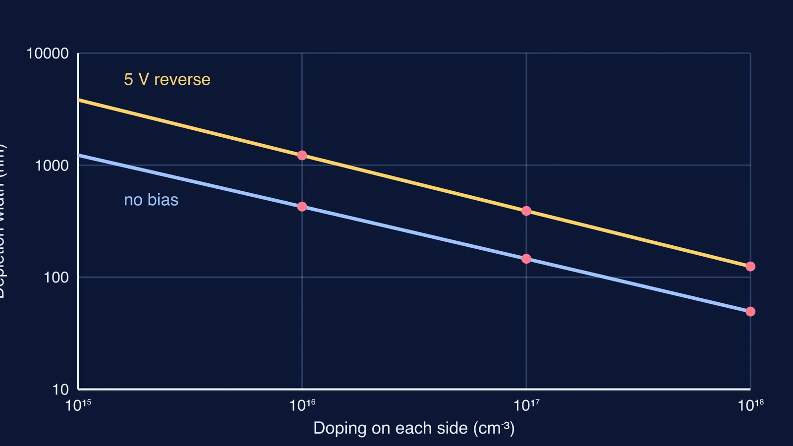
N = 10¹⁶ cm⁻³: Vbi ≈ 0.69 V and W ≈ 430 nm at zero bias. At 5 V reverse, W ≈ 1.2 µm and Emax ≈ 9 MV/m.
N = 10¹⁷ cm⁻³: Vbi ≈ 0.81 V and W ≈ 150 nm. At 5 V reverse, W ≈ 390 nm and Emax ≈ 30 MV/m.
N = 10¹⁸ cm⁻³: Vbi ≈ 0.93 V and W ≈ 49 nm. At 5 V reverse, W ≈ 125 nm and Emax ≈ 95 MV/m.
Each tenfold increase in doping cuts W by close to √10 ≈ 3.2 (about 2.9 at zero bias) and raises the field by a similar factor.
Why are Zener diodes heavily doped?
Breakdown happens when the junction field gets strong enough to drive a large reverse current. At the same 5 V, the 10¹⁸ cm⁻³ junction in the TU Graz-based example has about ten times the field of the 10¹⁶ cm⁻³ one. So a heavily doped junction reaches breakdown-level fields at a much lower reverse voltage.
ROHM, a semiconductor manufacturer, explains that Zener diodes "take advantage of the high electric field inside a heavily doped pn junction" (ROHM TechWeb). In many Zener diodes below about 5 to 6 V, the Zener effect, which relies on quantum tunnelling, dominates; higher-voltage diodes rely mostly on avalanche breakdown, where carriers gain enough energy to create new electron-hole pairs.
The effect is named after Clarence Zener, whose 1934 paper set out a theory of the electrical breakdown of solid dielectrics (Proceedings of the Royal Society A).
Lighter doping gives a wider layer and a higher breakdown voltage, which suits a rectifier diode: NCERT notes its reverse breakdown voltage must be sufficiently higher than the peak AC voltage (NCERT Chapter 14).
How do you answer this in a board or JEE question?
Answer in three steps:
Heavy doping packs many fixed ions into a small volume, so a thin layer balances the built-in potential (W scales as 1/√N).
The same voltage across a thinner layer gives a stronger electric field.
That field causes breakdown at a low reverse voltage, so a Zener diode can be made to hold a small, fixed voltage.
Two traps: saying heavier doping widens the layer, and forgetting the layer extends more into the lightly doped side. Doping sets the width at a given voltage; bias then changes it, as in how forward and reverse bias change depletion width. For the fixed ions, see why an n-type semiconductor is still neutral.
If you follow the reasoning but stumble when setting up the numbers, the Fermi Problem Library has worked problems with a step-by-step solver that explains the reasoning rather than printing an answer. For the ideas underneath, such as drift, diffusion and built-in potential, the Fermi Concept Library gives each concept its own lesson and its place in the map.
Try this next: redo the example with Na = 10¹⁸ and Nd = 10¹⁶ cm⁻³; almost all of W should sit on the n-side.