
On this page
When you start studying semiconductor electronics, the p-n junction is the first major hurdle. It is the building block of diodes, transistors and solar cells. To understand how these devices control the flow of electricity, we have to look at what happens the moment p-type and n-type semiconductors touch.
How does the depletion layer form by diffusion?
Imagine bringing a p-type semiconductor, which has a surplus of positively charged holes, into contact with an n-type semiconductor, which is packed with free electrons. Nature abhors a steep concentration gradient. Because of this gradient, electrons diffuse from the n-side to the p-side, and holes diffuse from the p-side to the n-side.
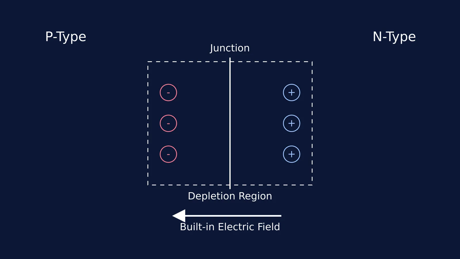
As these majority carriers cross the junction, they recombine. An electron drops into a hole, and both vanish as mobile charge carriers. However, the atoms they leave behind do not move. The p-side is left with negatively charged acceptor ions, and the n-side is left with positively charged donor ions.
This region of uncovered, fixed ions is swept clean of mobile charges, which is why it is called the depletion layer or depletion region. The depletion region is extremely thin, typically on the order of micrometers.
Why does drift oppose diffusion?
The separation of positive and negative fixed ions creates a built-in electric field that points from the n-side to the p-side. This field acts like a wall.
While diffusion tries to push more electrons to the p-side, the new electric field pushes them back. When the field is strong enough, it drives a drift current of minority carriers (electrons on the p-side and holes on the n-side) that flows in the exact opposite direction to the diffusion current.
If you struggle to picture these opposing invisible currents, the Fermi Simulation Lab has interactive simulations for the ideas that are easier to see than to read. You can watch the carriers build up the barrier until the drift current exactly balances the diffusion current. At this point of equilibrium, the net current across the junction is zero.
How does doping concentration affect the depletion layer?
The width of the depletion layer is not fixed; it depends heavily on how many impurities, or dopants, are added to the semiconductor. If one side of the junction is heavily doped, it has a high concentration of free charge carriers. Consequently, only a very thin slice of material needs to be depleted to uncover enough fixed ions to build the required barrier potential.
Conversely, a lightly doped region must be depleted deeper into the material to expose the same amount of fixed charge. In most practical diodes, one side is intentionally doped much more heavily than the other. This ensures that the depletion region extends almost entirely into the lightly doped side, which allows engineers to precisely control the electrical characteristics of the junction. For instance, in a p+ n junction, where the p-side is heavily doped, the depletion layer is found almost entirely on the n-side.
What is the barrier potential of a p-n junction?
The built-in electric field creates a potential difference across the junction, known as the barrier potential. This is the voltage you must overcome with an external battery (forward bias) to make the diode conduct. For a standard silicon p-n junction at room temperature, this barrier potential is approximately 0.7 V. For germanium, the barrier is lower, at about 0.3 V.
When you apply a forward bias, you are pushing against this barrier, narrowing the depletion region. If you apply a reverse bias, you reinforce the barrier, widening the depletion region and blocking current flow. You can read more about reading forward and reverse bias curves in our guide to The p-n junction diode: reading forward and reverse bias curves. Or, if you need to test your understanding of carrier mathematics, try these n-type and p-type semiconductors: carrier concentration problems.
Worked example: calculating the built-in electric field
To see why this barrier is so effective, let's calculate the electric field inside the depletion layer.
The problem: Suppose a silicon p-n junction has a typical barrier potential of 0.7 V and a depletion width of 1 micrometer. What is the magnitude of the built-in electric field?
The solution:
Use the relationship between voltage, electric field and distance for a uniform field: E = V / d
Substitute the values: E = 0.7 V / 10⁻⁶ m
Calculate the result: E = 7 × 10⁵ V/m
That is 700,000 volts per metre. It is a massive electric field packed into a microscopic space. This explains why minority carriers that wander into the depletion region are instantly swept across to the other side by drift.
If you find yourself stuck on the theory behind these calculations, the Fermi Concept Library has every concept in physics, chemistry, biology, mathematics and computing, each with its own lesson and its place in the map. If you want a wider overview of how energy gaps work in these materials, you can also explore how Energy bands: conductors, semiconductors and insulators compared govern the behaviour of solids.