
On this page
Almost every chip in your phone starts as a slice of one large crystal of silicon. The way that crystal is grown goes back to a slip of the hand in a Berlin laboratory in 1916.
What did Jan Czochralski discover in 1916?
Jan Czochralski, born in 1885 in Exin (now Kcynia, Poland), was an engineer at the electrical company AEG in 1916, according to his Wikipedia biography. He was looking for a way to measure how fast metals crystallise. While noting his observations, he dipped his pen into a crucible of molten tin instead of his inkwell.
When he pulled the pen out, a thin thread of solid tin hung from the nib. The Jan Czochralski memorial site describes what came next: experiments that evening showed that the speed of withdrawal changed the length and structure of the thread, and he swapped the pen for a glass tube and his hand for a clockwork mechanism. The Wikipedia biography adds that he verified the solidified metal was a single crystal.
His manuscript was received by the journal Zeitschrift für physikalische Chemie on 19 August 1916, the date now treated as the birth of the method, and was published in 1918 with results for tin, zinc and lead (janczochralski.com).
How did a metal experiment end up making chips?
At Bell Labs, chemist Gordon Teal argued that transistors needed large single crystals of germanium and silicon, and built the crystal-growing equipment with mechanical engineer John Little and technician Ernest Buehler, the Computer History Museum records. Building on Czochralski's technique, Teal suspended a small seed crystal in molten germanium and slowly withdrew it, forming a long, narrow single crystal.
The same museum page reports that William Shockley later called this achievement "the most important scientific development in the semiconductor field in the early days." Using the technique, chemist Morgan Sparks dropped tiny pellets of impurities into the melt as the crystal grew, building p-n junctions straight into it. If p-type and n-type are hazy, our explainer on doping in intrinsic and extrinsic semiconductors covers it.
How does the Czochralski method grow silicon today?
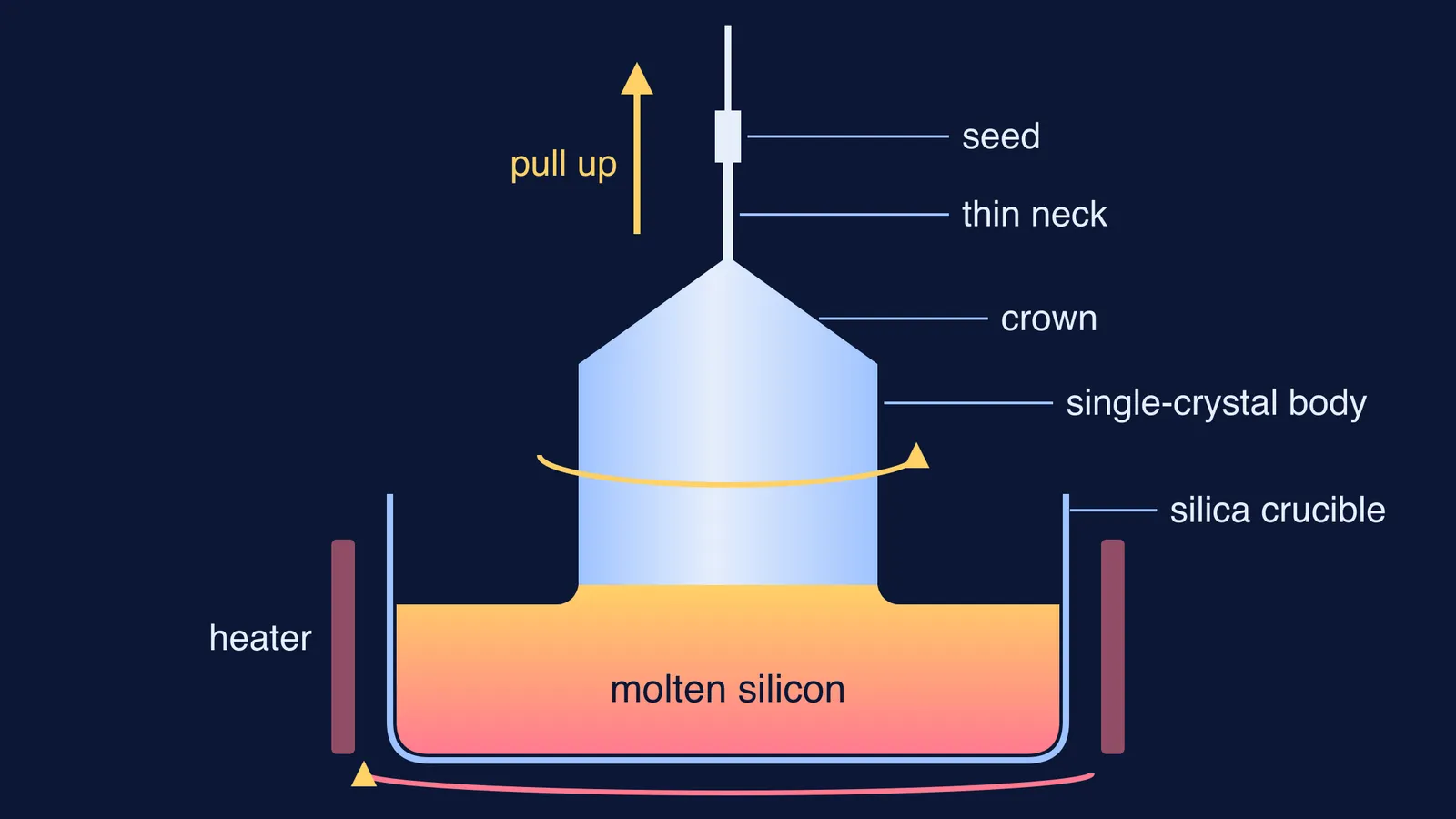
Silicon single crystals for electronics are produced mainly by the Czochralski method, in diameters of up to 300 mm, according to a chapter by Lukáš Válek and Jan Šik of ON Semiconductor. Their description of an industrial puller gives the steps:
Chunks of polysilicon go into a silica crucible inside a graphite hot zone, in a chamber filled with inert gas, usually argon.
The heater melts the charge, at about 1,425 °C (Wikipedia). Dopants such as boron or phosphorus can be added to the melt in precise amounts.
A seed crystal is lowered until it touches the melt.
Necking: the pull speeds up to about 3 to 6 mm per minute and the diameter shrinks to about 5 to 2 mm.
The crown: the pull slows and the crystal widens into a cone until it reaches the target diameter.
The body: the crystal grows as a cylinder, typically at or below 1 mm per minute. The crystal is rotated to even out impurities and temperature, and the crucible turns the opposite way to steady the melt flow.
The tail: the crystal narrows to a cone before leaving the melt, and is later cut, ground and sliced into wafers.
Worked example: how long does one silicon ingot take?
Take the typical body speed from Válek and Šik: at or below 1 mm per minute. Suppose you want a body 1 metre long (our assumption).
Time = length ÷ speed = 1,000 mm ÷ 1 mm per minute = 1,000 minutes.
1,000 ÷ 60 ≈ 16.7 hours at that top typical speed, before the neck, crown, tail and cooling.
Why so slow? The same chapter explains that the heat released as silicon solidifies is conducted to the crystal surface and radiated away, and in longer ingots that conduction is reduced, so the pull must slow further. That is latent heat from your physics textbook, setting the pace of a factory.
Which school ideas does this connect?
Before an exam, check you can explain each of these in two sentences:
Latent heat of fusion, and why a freezing surface must keep losing heat to move forward.
Seed crystals: the same reason a seed helps in the copper sulphate crystallisation practical.
Doping with boron (p-type) and phosphorus (n-type).
How real crystals grow layer by layer, as in Ajit Ram Verma's photographs of growth spirals.
If one of these feels shaky, the Fermi Concept Library gives every concept in physics and chemistry its own lesson. For more practice with rate calculations like this one, the Fermi Problem Library has worked problems with a step-by-step solver that explains the reasoning rather than printing an answer.
Next time you pick up a phone, remember that it began with a pen dipped in the wrong pot.