
On this page
Ajit Ram Verma was born on 21 September 1921 at Dalmau in Uttar Pradesh, according to his biographical memoir published by the Indian National Science Academy. He studied at Allahabad University and became a physics lecturer at the University of Delhi in 1947. In 1950 a British Council scholarship took him to Professor S. Tolansky's group at Royal Holloway College, University of London, known for multiple-beam interferometry, a way of using light to measure very small heights.
Tolansky suggested he study metal surfaces, a safe route to a PhD in about two years. But Verma had brought crystals from India, including haematite and silicon carbide (carborundum) with flat, shining faces. The memoir records that Tolansky finally agreed that "he can play with his crystals for some time".
Why did crystal growth need screw dislocations?
In the late 1940s the usual picture was that each new crystal layer starts as a tiny flat island of atoms. As the INSA memoir explains, F. C. Frank and co-workers showed that such islands almost never survive at low supersaturation, so crystals should barely grow. Real ones grew fine.
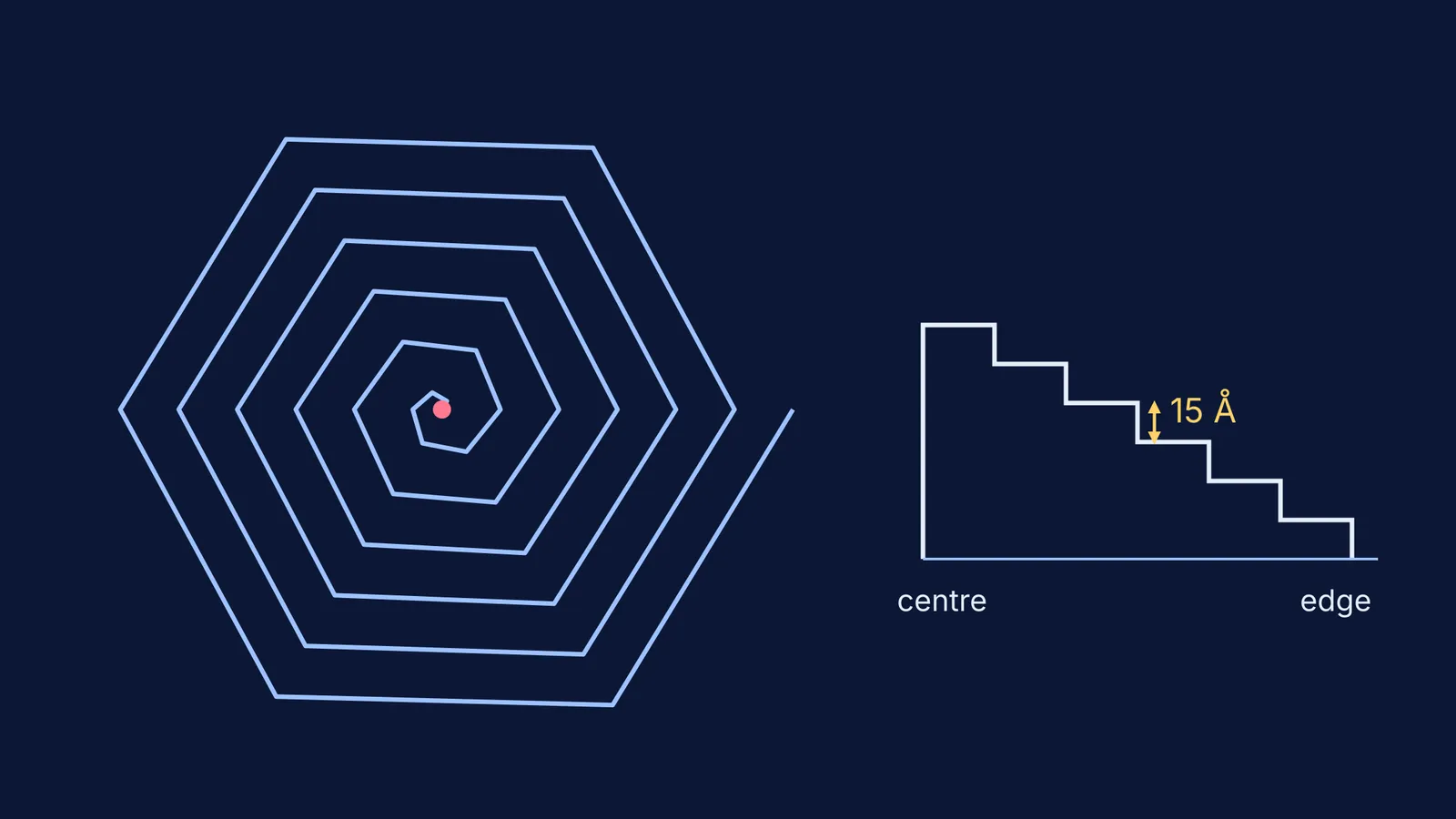
Frank's answer, in a 1949 paper in Discussions of the Faraday Society, was the screw dislocation. A screw dislocation is a defect in which the atomic layers of a crystal are joined like a spiral ramp, so where it meets the surface it leaves a step that never runs out. As atoms add to that step, it winds round the dislocation into a low spiral staircase.
The theory made two checkable predictions. The step height should match the unit cell (the smallest repeating block of the crystal) in that direction, and the spiral's shape should follow the symmetry of the face.
How did Verma see growth spirals on crystals?
Tolansky's lab had a phase contrast attachment for its Vickers projection microscope that was not in much demand. Phase contrast, invented by Frits Zernike, turns tiny differences in the path of light into differences in brightness; you can read how Zernike's phase contrast microscope works in our earlier piece. With it Verma saw a faint spiral on one of his silicon carbide crystals. According to the INSA memoir, his fellow students could not see it and suggested he photograph it, and the photograph proved him right.
He reported the spirals in Nature on 9 June 1951. In a longer paper in the Philosophical Magazine in September 1951, he described coating the crystal faces with a thin silver film of reflectivity nearly 90 percent and viewing them in reflected light with phase contrast. The spirals ranged from circular to regular hexagonal, in line with Frank's theory.
Why did the 15 ångström step height matter?
One ångström (Å) is 10^-10 metres. The INSA memoir gives the unit cell height of the common 6H form of silicon carbide as 15.1 Å. Verma pushed multiple-beam interferometry to its limit and measured the spiral steps at 15 ± 2 Å.
A second note in Nature in September 1951 sorted the spirals into two classes: those whose step height equals one unit cell, and those whose step height is a multiple of it.
Textbooks such as Charles Kittel's reproduced the spirals, and the memoir records that Linus Pauling wrote to Verma in 1957 calling his Royal Society paper on dislocations in silicon carbide crystals "an important contribution to our understanding of the structure and growth of crystals." Verma later built schools of crystallography at Delhi, Banaras Hindu University and the National Physical Laboratory, which he directed from 1965 to 1982.
How can you check a result the way Verma did?
Verma's method, with numbers from the INSA memoir, works for a school practical too:
Write the prediction as a number. Frank's theory predicted a step of one unit cell: 15.1 Å for 6H silicon carbide.
Compare using the error bar. 15 ± 2 Å means anything from 13 to 17 Å, and 15.1 sits inside it.
Measure everything on the same sample. At his PhD viva, J. D. Bernal asked how the step heights matched X-ray unit cells measured on different specimens; Verma later made both measurements on the same crystals in Bernal's lab at Birkbeck College.
A worked example: a step of 30 ± 2 Å, divided by 15.1 Å, gives 1.85 to 2.12 unit cells, so it is a two-cell spiral of the second class. A step of 22 ± 2 Å gives 1.32 to 1.59, and no whole number fits. Check the measurement and the sample before blaming the theory: the memoir reports that in some silicon carbide polytypes the measured steps were fractions of the unit cell, a puzzle that needed much more work.
If the unit cell still feels abstract, the Fermi Concept Library gives each concept in physics and chemistry its own lesson, and the Fermi Simulation Lab has interactive simulations for ideas that are easier to see than to read.
Read next: Lawrence Bragg and the X-ray law that maps atoms in crystals and Nicolaus Steno and the constant angles of crystal faces.