
On this page
A timing diagram question gives you two square waves, A and B, and asks you to sketch what comes out of a gate. It looks like a drawing problem, but it is really a truth-table problem repeated a few times. Once you cut the time axis into the right pieces, each piece is quick.
How do you find the output waveform from a timing diagram?
Use the same steps for every two-input gate:
Draw a light vertical line at every moment where A or B changes level. Between two neighbouring lines, both inputs are constant.
In each interval, write the pair of input levels as bits, for example (1, 0).
Apply the gate's rule to that pair to get one output bit per interval.
Draw the output as a flat line at that level across the interval, with a vertical step only at a line where the output bit changes.
Check: the output may only change at one of the lines you drew in step 1. A step anywhere else is an error.
Step 1 is the one people skip, and it is where most wrong answers start.
What are the rules for AND, OR, NAND and NOR?
A NAND gate performs the Boolean function Y = NOT(A·B), as stated in the Texas Instruments SN74HC00 quad NAND gate datasheet. A NOR gate performs Y = NOT(A+B), as stated in the Texas Instruments SN74HC02 quad NOR gate datasheet. In words:
AND: output high only when A and B are both high.
OR: output low only when A and B are both low.
NAND: the opposite of AND, so output low only when both inputs are high.
NOR: the opposite of OR, so output high only when both inputs are low.
If the rules feel shaky, the Fermi Concept Library gives each concept its own lesson, so you can revise truth tables before drawing.
Worked example: six intervals, four outputs
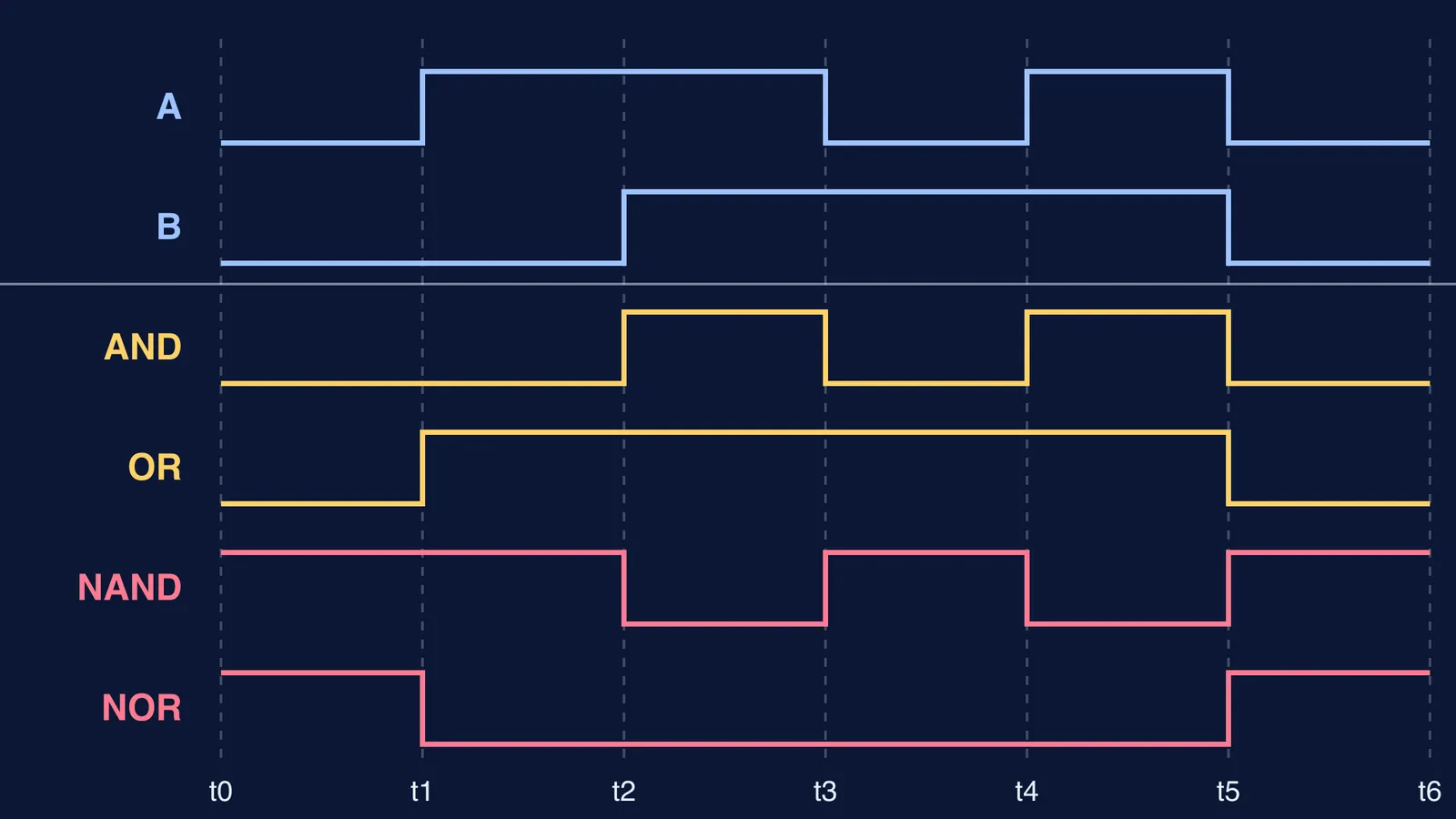
Take six equal intervals, t0 to t6, with these inputs:
A: 0, 1, 1, 0, 1, 0
B: 0, 0, 1, 1, 1, 0
Apply the rules to each pair:
t0 to t1, (0, 0): AND 0, OR 0, NAND 1, NOR 1
t1 to t2, (1, 0): AND 0, OR 1, NAND 1, NOR 0
t2 to t3, (1, 1): AND 1, OR 1, NAND 0, NOR 0
t3 to t4, (0, 1): AND 0, OR 1, NAND 1, NOR 0
t4 to t5, (1, 1): AND 1, OR 1, NAND 0, NOR 0
t5 to t6, (0, 0): AND 0, OR 0, NAND 1, NOR 1
So AND is 0, 0, 1, 0, 1, 0: two separate pulses. OR is 0, 1, 1, 1, 1, 0: one long pulse from t1 to t5. Notice that OR does not dip at t3 even though A falls there, because B is already high. NAND is 1, 1, 0, 1, 0, 1 and NOR is 1, 0, 0, 0, 0, 1. The diagram above draws all six rows.
What mistakes cost marks in these questions?
Marking the edges of only one input. Every edge of A and every edge of B starts a new interval.
Inverting the inputs instead of the output. NAND means AND first, then invert. Inverting A and B first and then ANDing them gives NOR, not NAND (that is De Morgan's law).
Extra steps. If neither input changes, the output cannot change.
Drawing delays that were not asked for. Real chips switch slightly late: the SN74HC00 datasheet lists a typical propagation delay of 9 ns at a 4.5 V supply and 25 °C. Exam diagrams assume ideal gates, so outputs switch exactly at input edges unless a delay is given.
For theory, see semiconductors and logic gates. Solving logic gate combination circuits applies this method one gate at a time, and how NAND builds NOT, AND and OR explains why NAND alone is enough.
Practice diagram: can you draw these four outputs?
On squared paper, sketch these inputs over eight equal intervals, t0 to t8:
A: 1, 0, 0, 1, 1, 0, 1, 0
B: 1, 1, 0, 0, 1, 1, 0, 0
Draw the four outputs below them, then check.
Answer, interval by interval:
AND: 1, 0, 0, 0, 1, 0, 0, 0
OR: 1, 1, 0, 1, 1, 1, 1, 0
NAND: 0, 1, 1, 1, 0, 1, 1, 1
NOR: 0, 0, 1, 0, 0, 0, 0, 1
If an interval is wrong, recheck the pair of bits you wrote for it first. For more practice, the Fermi Problem Library has worked problems with a step-by-step solver that explains the reasoning rather than printing an answer.
Redo the practice diagram tomorrow without looking at the rules.