
On this page
When you walk from a dim study into bright sunlight, your phone screen shifts almost instantly to maximum luminance. Tucked into the bezel or beneath the OLED panel is an ambient light sensor (ALS). As we explored in how a phone touchscreen senses your finger, phones pack dense solid-state physics behind the glass. At the sensor's core sits a semiconductor photodiode—a p-n junction engineered to turn incoming light into electric current through the internal photoelectric effect.
Where is the ambient light sensor, and how does it detect photons?
In modern sensors, such as the Texas Instruments OPT3001 ambient light sensor, incoming photons strike a silicon photodiode. In silicon, valence electrons are bound across an energy band gap of approximately 1.12 electron-volts (eV). Under dark conditions, thermal energy alone frees very few charge carriers.
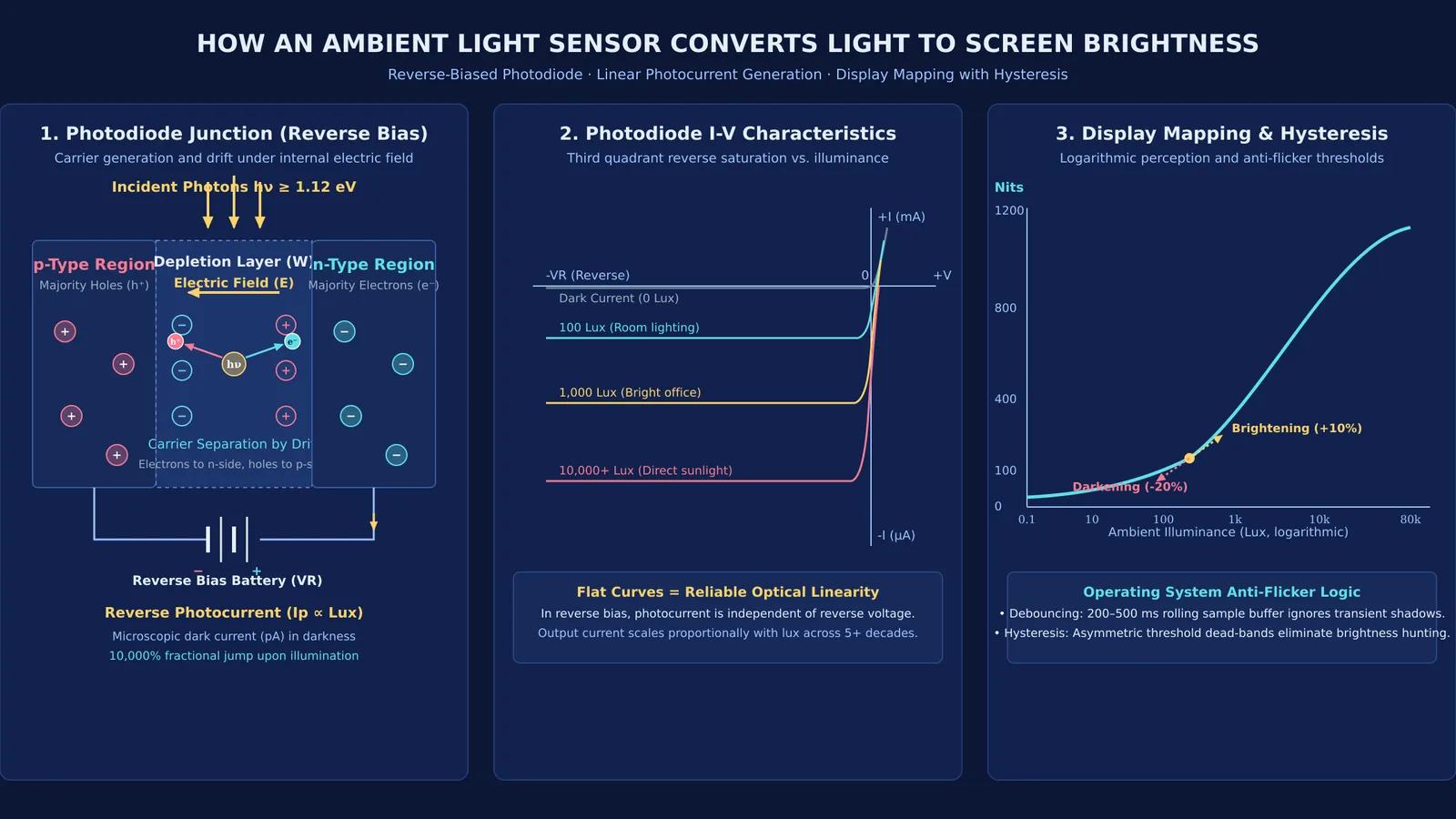
When light strikes the sensor aperture, photons carry energy E = hν. If photon energy exceeds the band gap (hν ≥ 1.12 eV), each absorbed photon excites an electron into the conduction band, leaving behind a vacant hole. This optical absorption creates an electron-hole pair. But detecting those newly liberated carriers requires a specific circuit configuration.
Why must the photodiode operate in reverse bias?
In CBSE Class 12 physics and JEE Main, examiners frequently ask why a photodiode operates in reverse bias rather than forward bias. While ambient light sensors optimize visibility across varying illumination as detailed in the Analog Devices technical analysis on ambient light sensing, the fundamental reason in semiconductor physics lies in carrier statistics and fractional change.
In forward bias, applied voltage floods the junction with millions of majority carriers—electrons in n-type silicon and holes in p-type silicon. Any light-generated pairs are lost in this massive baseline current.
Reverse bias does the opposite. Connecting the p-side to the negative terminal and the n-side to the positive terminal widens the depletion layer. As discussed in our guides on how depletion layer width changes in forward and reverse bias and how diffusion and drift build the depletion layer, this establishes an intense electric field pointing from the n-side to the p-side.
In darkness, only a microscopic dark current of minority carriers flows, typically in picoamperes (10⁻¹² A). When light strikes the depletion layer, the electric field sweeps electrons to the n-side and holes to the p-side before they recombine, producing a reverse photocurrent (I_p) proportional to illuminance.
Consider an n-type layer with majority electron density n = 10¹⁶ cm⁻³ and minority hole density p = 10⁸ cm⁻³. Suppose light generates excess pairs Δn = Δp = 10¹⁰ cm⁻³:
Forward bias fractional change: Δn / n = 10¹⁰ / 10¹⁶ = 10⁻⁶, or 0.0001%.
Reverse bias fractional change: Δp / p = 10¹⁰ / 10⁸ = 100, which is a 10,000% jump over baseline.
That 10,000% increase makes the signal immediately detectable.
How does the phone translate raw photocurrent into lux and nits?
As detailed in the Texas Instruments OPT3001 ambient light sensor specification, silicon absorbs near-infrared radiation up to 1,100 nanometres (nm), whereas human vision follows the CIE 1931 photopic curve peaking at 555 nm and dropping to zero beyond 700 nm. Without optical filtering, an incandescent bulb or ambient heat source would fool the sensor into over-brightening the screen in a dark room.
Precision sensors integrate optical filters that reject over 99% of infrared light. This allows accurate measurement from 0.01 lux in moonlight up to 83,000 lux in direct sunlight across a 23-bit effective dynamic range.
An on-chip transimpedance amplifier and analog-to-digital converter convert this photocurrent into a digital value. The Android Developer sensor framework reports this through `Sensor.TYPE_LIGHT` in SI lux units.
The display driver maps ambient lux to screen luminance in nits. As Prashanth Holenarsipur explains in an Analog Devices technical report on ambient-light sensing, human perception is logarithmic. The system uses an interpolation curve to keep screen power low indoors (50 to 150 nits for 300 lux) while driving displays to 800 or 1,200 nits outdoors. In experiments published in the European Journal of Physics, researchers confirmed that smartphone light sensors track illuminance accurately down to classical inverse-square law predictions.
Why does your screen not flicker when a shadow passes?
To prevent erratic jumping when a shadow passes, mobile operating systems apply software safeguards implemented in the Android Open Source Project display controller:
Debouncing: The system averages lux readings over a rolling window of 200 to 500 milliseconds to ignore momentary shadows.
Hysteresis: Ambient light must cross a higher threshold to brighten the screen, and drop below a separate, lower threshold to dim it.
Brightness is then adjusted smoothly over several hundred milliseconds so your pupils can adapt comfortably.
Connecting textbook semiconductor theory to daily hardware
Every time your phone dims at night or brightens outdoors, it executes the laws of carrier generation and minority drift. Visualising how charge carriers separate across a depletion barrier is far easier when you can test the variables yourself.
In the Fermi Simulation Lab, you can manipulate carrier densities, reverse voltages, and electric fields to observe how p-n junctions behave interactively. When solving diode or photoelectric numericals, the Fermi Problem Library breaks down multi-step physics solutions with complete reasoning for each step.