
On this page
Who invented flash memory?
Dr. Fujio Masuoka, an engineer at Toshiba, invented flash memory in the early 1980s, as recorded in his biographical profile. Before his work, electronic devices had to choose between volatile dynamic RAM that lost its contents when powered down and ultraviolet-erasable read-only memory (UV-EPROM) that required removing the chip and exposing it under ultraviolet light to clear data. Early electrically erasable chips (EEPROM) existed, but they required two transistors per bit and erased data byte by byte, making them slow and expensive.
Masuoka realised that erasing memory in large sectors with a single electrical pulse allowed each cell to use only one transistor. When his colleague Shoji Ariizumi observed an entire array clearing instantly, he noted it erased as fast as a camera strobe, giving the technology its name. Masuoka filed the foundational Japanese patent in 1980, followed by US Patent 4,531,203, laying the groundwork for solid-state storage.
How did Fujio Masuoka invent NOR and NAND flash?
Masuoka unveiled his first design at the IEEE International Electron Devices Meeting (IEDM) in San Francisco in December 1984. His team's 1984 IEDM paper demonstrated a 256K-bit memory array using 2.0 µm lithography and triple-polysilicon technology. This architecture, known as NOR flash, connected cells in parallel. It provided quick random access, making it well-suited for processor firmware and boot code, but each cell needed its own contact, limiting density.
To replace magnetic disks, Masuoka designed a denser configuration. In December 1987, Masuoka, Masaki Momodomi, Yoshihisa Iwata, and Riichiro Shirota presented their 1987 IEDM paper introducing NAND flash. By linking cells in series strings that shared bit-line contacts, NAND cut the number of contacts by approximately 80% and reduced cell area per bit by 30% to 6.43 µm² on 1.0 µm process rules. That compaction made pen drives, memory cards, and solid-state drives affordable.
How does a floating-gate transistor store data without power?
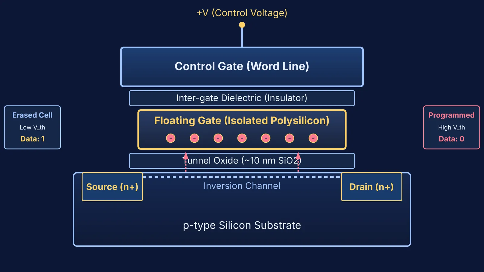
A flash cell adapts the metal-oxide-semiconductor field-effect transistor explained in how basic transistors switch. Between the control gate and the silicon channel, it embeds an electrically isolated conductor called a floating gate.
Silicon dioxide surrounds the floating gate, establishing an energy barrier across energy bands in conductors, semiconductors and insulators. Applying a high programming voltage forces electrons through this thin oxide layer via Fowler-Nordheim quantum tunnelling, as analysed in the 1987 IEDM paper. Once trapped, these electrons remain insulated without external electrical power.
Trapped charge shifts the cell's threshold voltage (ΔVth) according to the electrostatic relationship between stored charge and gate capacitance:
ΔVth = ΔQ / Ccg
Here ΔQ is the stored charge and Ccg is gate capacitance. For 1,000 electrons and a capacitance of 0.10 femtofarads (1.0 × 10⁻¹⁶ F):
ΔQ = 1,000 × (1.6 × 10⁻¹⁹ C) = 1.6 × 10⁻¹⁶ C
ΔVth = (1.6 × 10⁻¹⁶ C) / (1.0 × 10⁻¹⁶ F) = 1.6 V
This 1.6 V shift allows a sensing circuit to detect whether the cell is erased (logic 1, conducting) or programmed (logic 0, non-conducting).
If you want to visualise how quantum tunnelling and electric fields behave in semiconductor layers, the Fermi Simulation Lab provides interactive simulations for the ideas that are easier to see than to read.
Why was Toshiba slow to recognise the invention?
Toshiba was initially slow to develop Masuoka's breakthrough. In the early 1980s, Japanese manufacturers focused heavily on dynamic RAM. Executives saw little reason to fund an unproven non-volatile memory, so Masuoka conducted much of his initial work after hours. Intel read Masuoka's 1984 paper, recognised its value, and launched the first commercial NOR flash chips in 1988.
Frustrated by administrative assignments that pulled him from laboratory research, Masuoka left Toshiba in 1994 to teach at Tohoku University. In March 2004, he filed a lawsuit regarding patent compensation. In July 2006, the Tokyo District Court brokered a settlement in which Toshiba agreed to pay him 87 million yen, as cited in his biographical record. He received the 1997 IEEE Morris N. Liebmann Memorial Award and later the 2018 Honda Prize for his work.
What can engineering students learn from Masuoka's persistence?
Masuoka's story shows the power of challenging established assumptions. Where others treated byte-by-byte erasure as an unchangeable constraint, Masuoka questioned the premise. Similar to John Bardeen's work on the transistor, rethink boundary conditions when solving hardware problems:
Architecture: NOR connects cells in parallel for random access; NAND strings them in series to cut bit-line contacts by 80%, as introduced in Masuoka's 1987 IEDM paper.
Cell area: NAND's shared contacts allow higher storage capacity per square millimetre.
Real-world roles: NOR flash stores boot firmware; NAND flash stores files, photos, and applications in phones and SSDs.
When you work through semiconductor physics problems or circuit calculations, the Fermi Problem Library offers worked problems with a step-by-step solver that explains the reasoning rather than printing an answer.