
On this page
Every phone, laptop and calculator runs on transistors, yet many students meet them only as a symbol with three legs. This post explains what a bipolar junction transistor does, works one switch and one amplifier through with numbers, and is honest about which exams still ask about it.
Is the transistor still in my syllabus?
Probably not as a tested topic. The current NCERT chapter Semiconductor Electronics still mentions the bipolar junction transistor in its introduction, but its sections end with the junction diode as a rectifier. The CBSE 2026-27 physics curriculum stops at the diode rectifier too. The JEE (Main) 2026 syllabus and the NEET (UG) 2026 syllabus list diodes, LEDs, photodiodes, solar cells, the Zener diode and logic gates, but not transistors. If your board or a future syllabus includes it, this post gives you the basics; check the current year's document.
It is still worth an hour. Logic gates, which those syllabi do include, are built from transistors, and the idea of a small signal controlling a large one is at the heart of electronics. Our revision guide to semiconductors and logic gates covers the tested parts.
What is a transistor, and who discovered it?
The 1956 Nobel Prize in Physics went jointly to William Shockley, John Bardeen and Walter Brattain "for their researches on semiconductors and their discovery of the transistor effect".
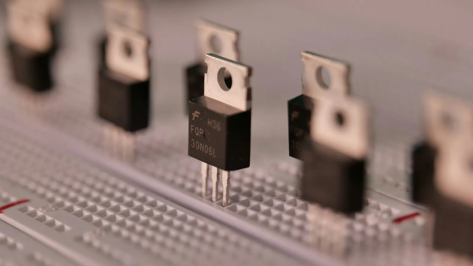
HyperPhysics, a physics reference from Georgia State University, describes the bipolar junction transistor as three regions of doped semiconductor. In an npn transistor, a p-type base sits between an n-type emitter and an n-type collector. A small current into the base controls a much larger current between collector and emitter:
I_C = β I_B, and the emitter carries both: I_E = I_B + I_C.
The current gain β is large, but it is not a fixed number. HyperPhysics gives a range of 20 to 200 and notes that it varies even for one transistor, with current and temperature. It adds two rules of thumb: about 0.6 V across the base-emitter junction "turns on" the transistor, and that voltage then changes very little.
What are the three operating states?
HyperPhysics lists three conditions:
Cut-off: no base current, so no collector current. The transistor is an open switch.
Active region: collector current follows I_C = βI_B. This is where it amplifies.
Saturation: the collector sits only a few tenths of a volt above the emitter and a large current flows. The transistor is a closed switch.
Worked example 1: a transistor as a switch
A 5 V digital output must switch a 1.0 kΩ load connected between a 5 V supply and the collector of an npn transistor. The datasheet gives β between 20 and 200. Choose the base resistor R_B.
Collector current when on. In saturation, take V_CE ≈ 0.2 V (a few tenths of a volt). I_C = (5 − 0.2) ÷ 1000 = 4.8 mA.
Base current needed. Design for the worst case, β = 20: I_B = 4.8 mA ÷ 20 = 0.24 mA.
Largest allowed R_B. The base-emitter junction takes about 0.6 V, leaving 5 − 0.6 = 4.4 V across R_B. R_B ≤ 4.4 V ÷ 0.24 mA ≈ 18 kΩ.
Pick a safe value. With R_B = 10 kΩ, I_B = 4.4 ÷ 10 000 = 0.44 mA, nearly twice what is needed, so the transistor saturates even with a low-gain part.
This follows the HyperPhysics advice on transistor switches: the base resistor must be small enough to drive the transistor into saturation. That page also notes that with the output taken at the collector, the switch inverts the input, which is a NOT gate.
Worked example 2: a transistor as an amplifier
A transistor with β = 100 has a 2.2 kΩ collector resistor and a 9.0 V supply. It is biased at I_B = 20 μA. A signal makes the base current swing by ±10 μA. Find the collector current and V_CE swings.
Resting point. I_C = 100 × 20 μA = 2.0 mA. V_CE = 9.0 − (2.2 kΩ × 2.0 mA) = 9.0 − 4.4 = 4.6 V.
Signal peaks. At I_B = 30 μA, I_C = 3.0 mA and V_CE = 9.0 − 6.6 = 2.4 V. At I_B = 10 μA, I_C = 1.0 mA and V_CE = 9.0 − 2.2 = 6.8 V.
Check the region. V_CE stays well above a few tenths of a volt, so the transistor never saturates and the output is not clipped.
Result. A 20 μA peak-to-peak base signal becomes a 2.0 mA collector swing and a 4.4 V swing in V_CE. The output is inverted: more base current means lower V_CE.
The emitter current at rest is 2.0 + 0.02 = 2.02 mA, so the collector carries about 99% of it, which matches the HyperPhysics description of normal transistor action.
Which mistakes come up?
Treating β as a constant. HyperPhysics warns that a circuit that depends on one exact β is a bad circuit. Design with margins.
Forgetting the 0.6 V drop. The full input voltage does not appear across R_B.
Assuming the amplifier output is in phase. In this common-emitter set-up it is inverted.
Ignoring saturation in amplifier questions. Always check that V_CE stays above a few tenths of a volt at the signal peaks.
If the idea of holes and electrons crossing junctions is the shaky part, the Fermi Concept Library covers every concept in physics, each with its own lesson, so you can revisit p-n junctions before transistors.
A practice routine
Day 1: Draw npn and pnp symbols and label E, B and C, with current arrows.
Day 2: Redo Worked example 1 for a 12 V supply and a 470 Ω load.
Day 3: Redo Worked example 2 with a 3.3 kΩ resistor and find the largest base swing before saturation.
Day 4: Explain in five sentences how one transistor makes a NOT gate.
This week, sketch a transistor switch driving an LED and calculate its base resistor using the worst-case β.