
On this page
Until the late 1970s, designing a silicon microchip was an artisanal craft restricted to semiconductor manufacturers. Designing an integrated circuit required working inside corporate fabrication lines, wrestling with proprietary chemical recipes. Conway had previously invented dynamic instruction scheduling at IBM in the 1960s (Smotherman and Spicer 2010), but testing experimental processor architectures required direct access to silicon without mastering device physics and photolithography first.
Rapidly rising component density created a crisis. As transistor counts compounded, reaching approximately 20,000 transistors on a single chip by 1978, device physicists building fabrication lines were rarely computer architects. Understanding how semiconductors form logic gates and managing carrier concentrations in n-type and p-type silicon remained locked inside specialized industrial teams.
Why was microchip design so difficult before 1978?
Before 1978, layout rules filled thick binders with hundreds of process-dependent tolerances in absolute micrometres, each tied to a specific factory's optical aligners. Whenever a manufacturer updated its lithography tools, existing mask layouts became obsolete.
Draftsmen spent months redrawing thousands of shapes on Mylar sheets with rubylith cutters. As Lynn Conway explained in the *IEEE Solid-State Circuits Magazine*, this tight coupling between circuit architecture and physical fabrication created a severe bottleneck that threatened to stall computing progress.
How did Lynn Conway's lambda rules simplify chip layouts?
At Xerox PARC, working with Carver Mead of Caltech, Lynn Conway introduced a clean architectural abstraction. Instead of defining geometries in absolute micrometres, Conway formulated dimensionless layout rules governed by a single parameter: lambda (λ).
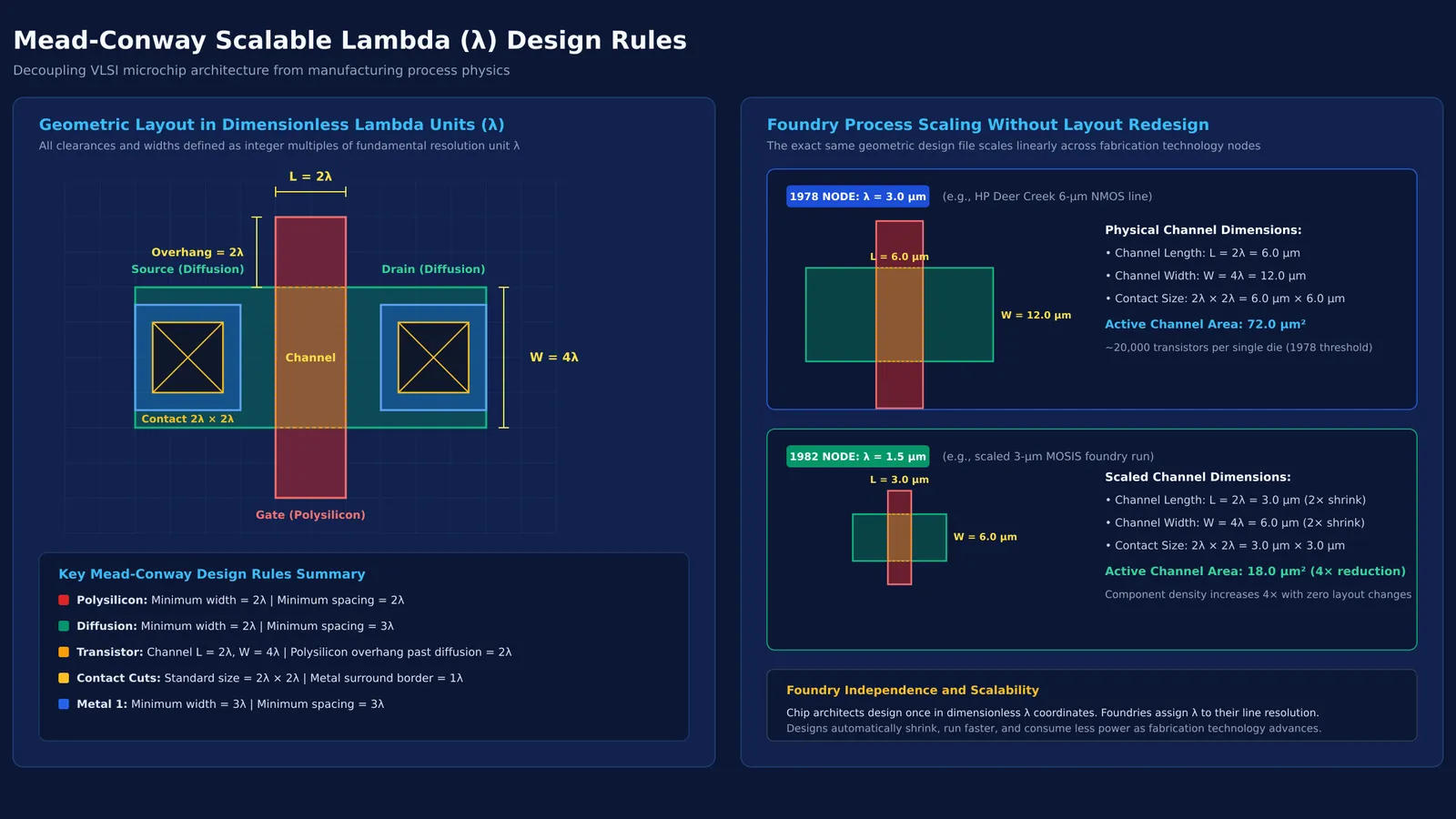
The parameter λ represents the fundamental resolution and alignment tolerance of the fabrication line—typically half the minimum transistor channel length. Under Conway's rules, published in *Introduction to VLSI Systems*, every geometric clearance is an integer multiple of λ:
Polysilicon gate length and line width: 2λ
Polysilicon spacing: 2λ
Diffusion line width: 2λ; diffusion spacing: 3λ
Polysilicon extension past diffusion: 2λ (preventing edge leakage)
Metal interconnect width and spacing: 3λ
Contact cuts: 2λ × 2λ with 1λ metal border
Because designs used dimensionless units of λ, layouts became scalable. When a factory improved its lithography, software simply scaled λ, shrinking the entire geometry uniformly without manual redrawing.
What happened during the 1978 MIT course and MPC79?
To test whether students could design working silicon, Conway taught Course 6.978 at MIT in autumn 197890054-0). In the first six weeks, students learned MOS principles and lambda rules. During the final six weeks, they designed custom microchips.
Conway had student design files, formatted in Caltech Intermediate Form (CIF), transmitted across the ARPANET to Xerox PARC. The designs were merged onto a multi-project mask set and fabricated at Hewlett-Packard's Deer Creek facility. In January 1979, students received working, packaged microchips, including Guy Steele's Scheme microprocessor.
Building on this success, Conway coordinated MPC79 in autumn 1979. As documented in the *Euromicro Journal*90054-0), 124 designers across 12 universities submitted 82 design projects90054-0) over the ARPANET by 4 December 1979. HP fabricated the wafers, returning working chips by January 1980. These included Jim Clark's Stanford geometry processor, published in *IEEE Computer*, which launched Silicon Graphics.
How did Mead-Conway methods create the fabless chip industry?
The multi-project chip showed that dozens of teams could share mask fabrication costs. In 1981, DARPA established MOSIS, turning Conway's network into a national prototyping service.
This separated the semiconductor industry into two distinct layers:
Fabless companies (such as ARM, NVIDIA, and Qualcomm) that design processors without owning fabrication facilities.
Pure-play silicon foundries (such as TSMC) focused entirely on manufacturing wafers.
According to the University of Michigan VLSI Archive, *Introduction to VLSI Systems* spread to more than 100 universities within a few years, establishing a common curriculum and standardizing layout conventions across academia and industry.
When connecting physical semiconductor principles to logic circuits, the Fermi Concept Library covers every concept in physics and computing, each with its own lesson and its place in the map. For students exploring energy bands in semiconductors and conductors, the Fermi Simulation Lab provides interactive simulations for ideas that are easier to see than to read.
How do you calculate transistor dimensions using lambda design rules?
In *Introduction to VLSI Systems*, Conway and Mead illustrated how lambda rules calculate dimensions for an nMOS transistor with a width-to-length ratio of W/L = 2:
Gate length: L = 2λ
Channel width: W = 4λ
Polysilicon extension past diffusion: 2λ (total strip length = 8λ)
Contact cut: 2λ × 2λ with 1λ metal border
Scaling across foundry nodes scales physical dimensions without redesigning layouts:
At λ = 3.0 μm (1978 node): gate length L = 6.0 μm, channel width W = 12.0 μm, and contact cut = 6.0 μm × 6.0 μm.
At λ = 1.5 μm (1982 node): gate length L = 3.0 μm, channel width W = 6.0 μm, and contact cut = 3.0 μm × 3.0 μm.
Transistor area shrinks by a factor of 4 (4×) without altering a single coordinate in the design file.
Students can apply Conway's four-step abstraction framework to complex STEM problems:
Separate interface from implementation: define what a block does before choosing how it is built.
Find the dimensionless scaling factor: express layout rules relative to a base parameter (like λ).
Build verified modular cells: test basic components before assembling large systems.
Automate verification: check constraints with software before final execution.