

On this page
Before 1959, early semiconductors had a fatal flaw. They were built by etching away silicon to leave a raised plateau, or "mesa", which stood above the rest of the wafer. This manufacturing process exposed the boundaries between n-type and p-type semiconductors directly at the edges of the structure.
When a p-n junction is exposed to the open air, it acts like a magnet for impurities. Dust, moisture, and stray ions from the manufacturing environment would settle on the raw silicon edge. These contaminants disrupted the delicate balance of electrons and holes at the junction.
This contamination created unwanted, highly conductive paths along the surface, leading to high reverse leakage currents. In practical terms, it meant the transistor would leak electricity even when it was supposed to be switched off. This made early computers and aerospace systems unreliable, as the transistors would degrade and fail unpredictably over time.
What is the planar process?
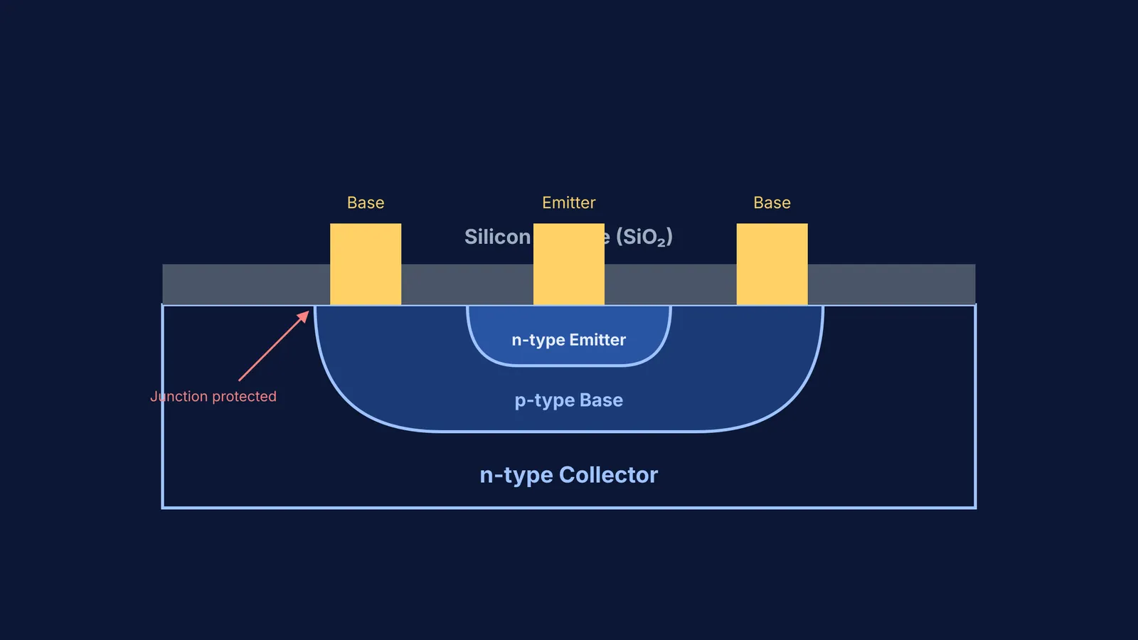
While working at Fairchild Semiconductor, Jean Hoerni had a simple but powerful idea that transformed semiconductor manufacturing. Instead of etching away the silicon dioxide (SiO₂) layer that was used as a temporary chemical mask during manufacturing, he decided to leave it in place permanently.
In Hoerni's planar process, dopants (the impurities that create p-type and n-type silicon) were diffused into the silicon wafer through small windows cut into the oxide mask. Because these dopant atoms spread sideways as well as straight down during the heating process, the edges of the newly formed p-n junctions ended up safely tucked underneath the protective oxide layer.
The silicon dioxide layer acted as a built-in hermetic seal. This process, known as surface passivation, protected the sensitive junctions from the environment and kept the overall surface of the chip entirely flat, or planar.
How much did the planar process reduce leakage?
The impact of the planar process was immediate and measurable. When Fairchild released the first commercial planar transistor, the 2N1613, in 1960, the difference in performance was clear.
The protective oxide seal reduced the transistor's leakage current by a factor of 1,000 compared to older mesa designs. Suddenly, transistors were no longer fragile, hand-crafted components; they were robust, reliable, and ready for mass production and critical military missions.
When learning the physics of semiconductors and energy bands, visualizing how charge carriers move across these junctions is often the hardest part. The Fermi Concept Library breaks down p-n junctions and depletion regions step by step, helping you see exactly why surface contamination causes unwanted current.
How to explain the planar process in an exam?
If you are asked to compare the mesa and planar processes in a physics or chemistry exam, use this three-point checklist to structure your answer:
Structure: The mesa process etches silicon away to leave a raised plateau, whereas the planar process leaves the silicon flat and covered with a silicon dioxide layer.
Junction protection: Mesa junctions are exposed at the surface and vulnerable to contamination. Planar junctions terminate underneath the silicon dioxide, which passivates and seals them from the air.
Outcome: The planar process drastically reduces leakage current and provides a flat insulating surface that allows metal interconnects to be drawn on top.
How did the planar process lead to the integrated circuit?
Hoerni's invention did more than just fix the transistor's leakage problem. By keeping the surface completely flat and insulated, the planar process provided the missing link for the next major step in computing.
Fellow Fairchild founder Robert Noyce realized that with a flat, insulating layer of oxide covering the entire silicon wafer, he could evaporate microscopic metal tracks directly on top of the chip to connect multiple transistors together. This insight—made possible entirely by Hoerni's flat oxide layer—resulted in the first practical monolithic integrated circuit.
Today, every microchip in our phones, cars, and laptops is still manufactured using the fundamental principles of Jean Hoerni's planar process.