
On this page
Every band diagram in your Class 12 semiconductor chapter rests on an idea Felix Bloch worked out as a PhD student in Leipzig in 1928. He showed that an electron in a crystal moves as a wave shaped by the repeating rows of atoms, and that its allowed energies come in bands. Here is how he got there, what he missed, and how to use it.
What problem was Felix Bloch trying to solve?
Bloch was born in Zurich in 1905, arrived in Leipzig in the autumn of 1927 to study under Werner Heisenberg, and took his PhD there in 1928, as he recalled in his memoir Memories of electrons in crystals. Heisenberg suggested he look into the theory of metals.
Physicists then treated conduction electrons as a gas of free particles. Bloch could not see how free motion was even roughly possible: a metal wire "with all its densely packed ions is far from being a hollow tube", he wrote.
He was sure the answer lay in the wave nature of the electron, the idea Louis de Broglie proposed in his PhD thesis. He also remembered a classroom demonstration: a row of coupled pendulums on a rod, where the swing of one would "migrate" along the row. The repeating pattern of a crystal, he sensed, would be essential.
How did Bloch explain energy bands in solids?
One evening in early January 1928, with pencil and paper, Bloch took one electron in a one-dimensional periodic potential, a potential energy that repeats with the spacing of the atoms. In his words: "By straight Fourier analysis I found to my delight that the solutions of the Schrödinger equation differed from the de Broglie wave of a free particle only by a modulation with the period of the potential" (Bloch, 1980).
An electron in a perfect crystal is a free-electron wave modulated by a pattern that repeats from one atom to the next. It belongs to the whole crystal, not to one atom.
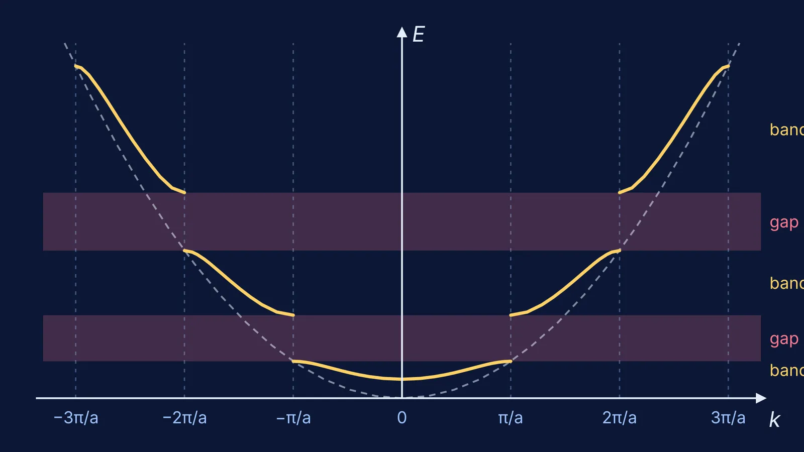
The thesis appeared in Zeitschrift für Physik, volume 52, pages 555-600, in 1929. Treating the lattice as a three-dimensional periodic potential, Bloch found that the allowed energy states "were not discrete, but were distributed in continuous bands", as his Lindau Nobel Laureate Meetings profile puts it.
In 1931 Kronig and Penney solved one such potential exactly. Their abstract opens: "Through the work of Bloch our understanding of the behaviour of electrons in crystal lattices has been much advanced" (Kronig and Penney, 1931). The diagram above comes from their model: inside a band a travelling wave exists for every energy; in a gap, none does.
Where do conductors, insulators and semiconductors come from?
Bloch did not take this step himself. He wrote that he "did not think of conduction bands in the sense in which they are now commonly understood", and that the essential difference between insulators and conductors was "later pointed out by A. H. Wilson" (Bloch, 1980). Wilson's paper, The theory of electronic semi-conductors, came out in 1931.
As Bloch put it, "closed shells have their analogue in filled bands". A full band, like a full shell, carries no current. In modern words:
Conductor: the highest band holding electrons is only partly full, or overlaps the empty band above, so electrons have empty states right next to them.
Insulator: that band is full, and the gap to the empty band above is large.
Semiconductor: the band is full, but the gap is small enough for heat or light to lift some electrons across.
Silicon's gap is 1.11 eV and germanium's is 0.66 eV at 300 K, according to NPTEL course notes on semiconductors. Our post on energy bands in conductors, semiconductors and insulators works through more examples.
How do you read a band diagram in a Class 12 answer?
Ask four questions:
Which is the highest band that holds electrons?
Is it full? Partly full, or overlapping the band above, means a conductor.
If full (the valence band), how wide is the gap above it? Small means a semiconductor, large an insulator.
What can lift electrons across? Heat or light. Doping instead adds levels near a band edge.
Worked example. What is the longest wavelength of light that can lift an electron across each gap (NPTEL values)? Photon energy is E = hc/λ, and hc = 1.23984 × 10⁻⁶ eV m, or 1239.84 eV nm (NIST CODATA).
Silicon: λ = 1239.84 eV nm ÷ 1.11 eV ≈ 1117 nm.
Germanium: λ = 1239.84 eV nm ÷ 0.66 eV ≈ 1879 nm.
Both lie in the infrared, beyond red light, so any visible photon carries enough energy to cross either gap. A smaller gap means a longer cut-off wavelength. For what doping does next, see our guide to n-type and p-type carrier concentration problems.
If a wave turning into a band still feels abstract, the Fermi Simulation Lab has interactive simulations for ideas that are easier to see than to read, and the Fermi Concept Library gives every physics concept its own lesson and its place in the map.
Bloch later shared the 1952 Nobel Prize in Physics for work on nuclear magnetic precision measurements (Lindau profile). His first idea is the one in your syllabus.