
On this page
In 1959, at Bell Labs, Mohamed M. (John) Atalla and Dawon Kahng made the first successful insulated-gate field-effect transistor, the device now called the MOSFET, according to the Computer History Museum. Here is who they were, what problem they cracked, and a calculation you can do with Class 12 capacitor physics.
Who invented the MOSFET, and when?
Atalla was born in Port Said, Egypt, earned his PhD at Purdue University in 1949 and then joined Bell Laboratories to study the surface of silicon, says his National Inventors Hall of Fame profile. Kahng took a bachelor's degree at Seoul National University in 1955, then a master's and doctorate at Ohio State University, and joined Bell Labs in 1959, according to his Hall of Fame entry. Atalla gave Kahng the task of building the device, and the pair announced it at a conference in 1960. Both were inducted into the Hall of Fame in 2009.
Kahng's patent, titled Electric Field Controlled Semiconductor Device, was filed on 31 May 1960 and granted on 27 August 1963 (US 3,102,230).
The idea itself was older. Julius Edgar Lilienfeld filed patents between 1925 and 1928 describing a field-effect element now recognised as an MOS transistor, the museum notes.
What problem did Atalla solve first?
The obstacle was surface states: states at the semiconductor's surface that blocked electric fields from getting into the material. Investigating silicon dioxide grown on silicon by heating, Atalla and Kahng found the oxide markedly reduced those states (Computer History Museum). Atalla, Tannenbaum and Scheibner published Stabilization of Silicon Surfaces by Thermally Grown Oxides in the Bell System Technical Journal in May 1959 (DOI record).
This step, surface passivation, is what the Hall of Fame calls a critical step that made possible the ubiquity of silicon integrated circuits.
How does a MOSFET work?
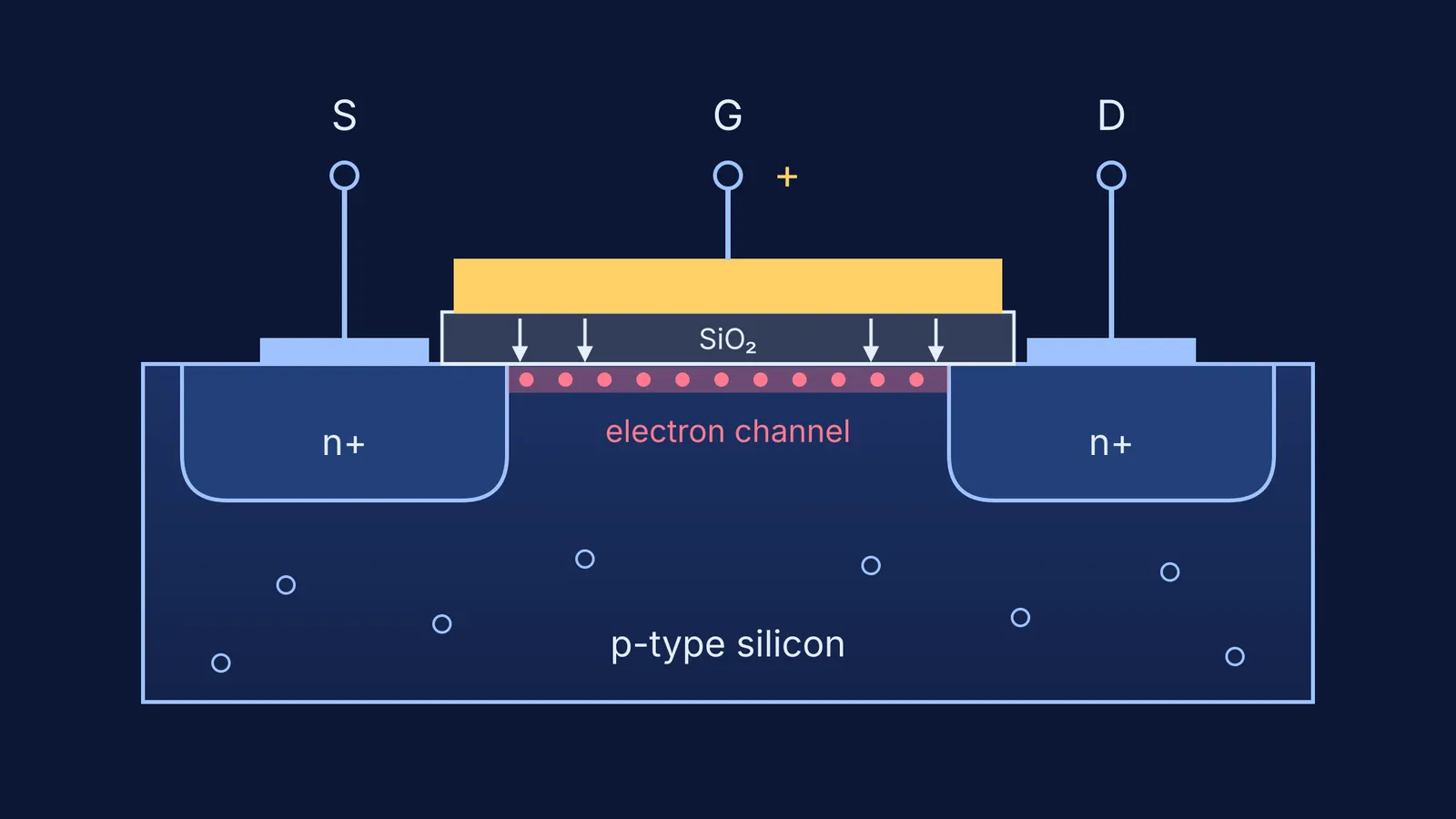
The name lists its layers: a metal gate (M), an insulating oxide (O) and the silicon semiconductor (S), as the Computer History Museum explains. In an n-channel MOSFET, two n-type regions, the source and the drain, sit in p-type silicon that forms a barrier for electrons between them (MIT 6.012, lecture 9). Put a positive voltage on the gate and electrons gather just under it. Once the gate-to-source voltage passes the threshold voltage, this inversion layer connects source and drain, and the transistor is on (Toshiba's explainer).
Why did a slow 1959 device end up in nearly every chip?
At first Bell Labs did not pursue it. The device was slow and addressed no pressing need of the telephone system, the Computer History Museum records. Yet in a 1961 memo, quoted there, Kahng pointed to its "ease of fabrication and the possibility of application in integrated circuits." Researchers at RCA and Fairchild built MOS devices in 1960, RCA made an experimental 16-transistor integrated device in 1962, and MOS devices reached the market in 1964.
In 1963 Frank Wanlass at Fairchild conceived and patented complementary MOS (CMOS), which in the museum's words "consumed zero power when not in use" (CHM blog). The same article cites analyst Jim Handy's updated estimate of 13 sextillion transistors made, and says 99.9 percent of them were MOS devices.
Over 99 percent of microchips produced today use MOS transistors, according to the Computer History Museum.
How many electrons does a MOSFET gate pull in?
Above threshold, the channel charge per unit area is q = C_ox(V_G − V_T), with the gate voltage V_G measured from the silicon body and C_ox the oxide capacitance per unit area (MIT 6.012, slide 15). C_ox = ε_r ε_0 / t_ox, and ε_r = 3.9 for silicon dioxide (gate capacitance).
Take a 10 nm oxide and a gate 1 V above threshold (illustrative values, not the 1959 device's):
C_ox = 3.9 × 8.854 × 10⁻¹² F/m ÷ 1.0 × 10⁻⁸ m ≈ 3.45 × 10⁻³ F/m².
Charge per area = 3.45 × 10⁻³ F/m² × 1 V = 3.45 × 10⁻³ C/m².
Electrons per area = 3.45 × 10⁻³ ÷ 1.602 × 10⁻¹⁹ ≈ 2.2 × 10¹⁶ per m².
One square micrometre is 10⁻¹² m², so that is about 22,000 electrons in each µm² of channel.
Now test yourself:
Double the oxide thickness, keeping the gate 1 V above threshold: C_ox halves, so the electron count halves.
Raise the gate to 2 V above threshold: the count doubles.
Hold the gate below threshold: no inversion channel forms, so the transistor stays off.
Where should you go next?
If bands still feel shaky, start with energy bands in conductors, semiconductors and insulators, then practise carrier concentration problems for n-type and p-type semiconductors. For the junction that came first, read how Russell Ohl's cracked silicon revealed the p-n junction.
If the capacitor step is where you get stuck, the Fermi Concept Library has a lesson for every concept in physics, chemistry, biology, mathematics and computing. The Fermi Simulation Lab has interactive simulations for ideas that are easier to see than to read.