
On this page
In the late 1970s at the Vavilov State Optical Institute in Leningrad, Soviet physicist Alexei Ekimov investigated coloured silicate glass. Artisans had long produced vivid ruby and amber glass by adding metal salts and adjusting furnace cooling schedules, but the underlying physics remained unknown. Ekimov introduced copper chloride (CuCl) into silicate glass and annealed samples between 500 °C and 700 °C for durations spanning 1 hour to 96 hours. When he cooled the glass to 4.2 K and recorded its optical absorption, smaller crystals absorbed light at shorter, bluer wavelengths.
Small-angle X-ray scattering revealed that heat treatment had grown CuCl nanocrystals with diameters from 2 nanometres to 30 nanometres. Crystals near 30 nm matched bulk copper chloride, but those near 2 nm shifted toward higher energies, as reported by Ekimov and Alexey Onushchenko in JETP Letters in 1981. This first observation of three-dimensional quantum confinement earned Ekimov the 2023 Nobel Prize in Chemistry alongside Louis Brus and Moungi Bawendi.
How did Alexei Ekimov grow and measure quantum dots?
Ekimov studied how crystalline phases precipitate inside an amorphous silicate glass melt. Copper and chlorine dissolved into molten glass at high temperatures. When held in a secondary furnace between 500 °C and 700 °C, the supersaturated ions diffused through the glass matrix and precipitated into solid semiconductor clusters by Ostwald ripening. Halting the furnace at different times froze crystal growth at specific sizes, while the rigid glass matrix isolated each nanocrystal from its neighbours.
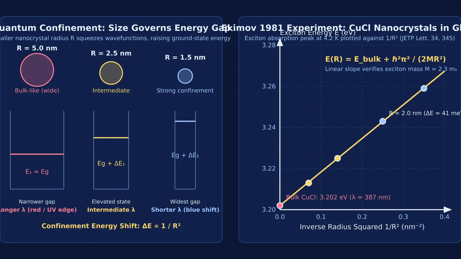
Small-angle X-ray scattering measured the crystal diameters without destroying the samples. Optical absorption spectroscopy showed that the exciton absorption peak of CuCl—fixed at 3.202 eV in bulk crystals—marched systematically to higher energies as crystal diameter shrank. Ekimov later reported these results in Solid State Communications in 198580025-9), demonstrating that physical dimensions modify electronic structure just as altering energy bands in semiconductors and insulators does through chemical doping.
Why does shrinking crystal size shift absorption to blue?
In bulk semiconductors, millions of atoms share electrons, forming valence and conduction bands separated by a fixed bandgap. Absorbing a photon promotes an electron to the conduction band, leaving a hole. Electrostatic attraction binds the pair into an exciton. In CuCl, the exciton Bohr radius is approximately 0.7 nanometres. When a crystal's radius R approaches this scale, the exciton is squeezed inside a three-dimensional potential well.
Quantum mechanics requires a particle's kinetic energy to rise as the confinement space contracts. Squeezing a particle into a smaller volume forces its momentum uncertainty to rise, raising its ground-state kinetic energy. This extra energy adds directly to the bulk bandgap, meaning that exciting an electron requires a higher-energy photon: a blue shift.
How does the Efros equation model quantum confinement?
Ekimov collaborated with Soviet theorists Alexander Efros and Alexei Efros, who published the mathematical framework in their 1982 theoretical model. In the weak confinement regime, where nanocrystal radius R exceeds the exciton Bohr radius, the exciton moves as a composite particle confined within a spherical box.
The exciton transition energy E(R) follows a quadratic scaling law: E(R) = Eg − Eex + [ℏ²π² / (2MR²)] Here, Eg is the bulk bandgap, Eex is exciton binding energy, ℏ is the reduced Planck constant, and M = me + mh is the exciton translational mass. When Ekimov plotted the measured absorption peak against 1/R², the points formed a straight line whose slope matched the known effective mass of CuCl.
Worked example: how do you calculate the blue shift for a CuCl nanocrystal?
Consider a CuCl nanocrystal with radius R = 2.0 nm, modeled using the Efros confinement framework:
Bulk baseline: Bulk CuCl at 4.2 K has an exciton absorption line at E_bulk = Eg − Eex = 3.202 eV.
Effective mass: For CuCl, translational mass M ≈ 2.3 m₀ ≈ 2.095 × 10⁻³⁰ kg, and ℏ = 1.055 × 10⁻³⁴ J·s.
Confinement shift:
ΔE = ℏ²π² / (2MR²) For R = 2.0 × 10⁻⁹ m, ΔE = [(1.055 × 10⁻³⁴)² × π²] / [2 × (2.095 × 10⁻³⁰) × (2.0 × 10⁻⁹)²] ≈ 6.55 × 10⁻²⁰ J. Dividing by 1.602 × 10⁻¹⁹ J/eV gives ΔE ≈ 0.041 eV (41 meV).
Shifted peak and wavelength: The new transition energy is E(R) = 3.202 eV + 0.041 eV = 3.243 eV. By converting between photon energy in electron-volts and wavelength in nanometres using λ = 1240 / E, the absorption edge shifts from 387.3 nm in bulk to 382.4 nm in the 2.0 nm nanocrystal: a 4.9 nm blue shift.
If the crystal shrinks to 1.2 nm, ΔE rises to 0.114 eV, shifting the absorption edge to 374 nm.
How can students connect quantum confinement to core physics?
For students preparing for competitive exams like JEE Advanced, quantum dots demonstrate that de Broglie matter waves and particle-in-a-box energy levels govern material colours, rather than existing only as abstract exercises.
If you find it difficult to visualise how shrinking a potential well forces wavefunctions into higher energy states, the Fermi Simulation Lab provides interactive simulations for ideas that are easier to see than to read. To explore how discrete energy levels emerge and compare nanoscale confinement to bulk band gaps, the Fermi Concept Library maps every concept in physics and chemistry, each with its own lesson and its place in the map. When solving problems on de Broglie wavelengths and particle-in-a-box energy shifts, the Fermi Problem Library offers worked problems with a step-by-step solver that explains the reasoning rather than printing an answer.