
On this page
When you reverse-bias a p-n junction diode, it normally blocks current flow until the voltage becomes too high. Beyond a certain threshold, the diode gives way, breaking down and allowing current to flow freely in the reverse direction. In semiconductor physics, this reverse breakdown happens in two entirely different ways: the Zener effect and avalanche breakdown.
The mechanism that dominates the breakdown depends almost entirely on how heavily the semiconductor is doped during manufacturing, and the specific voltage applied across it.
What causes Zener breakdown?
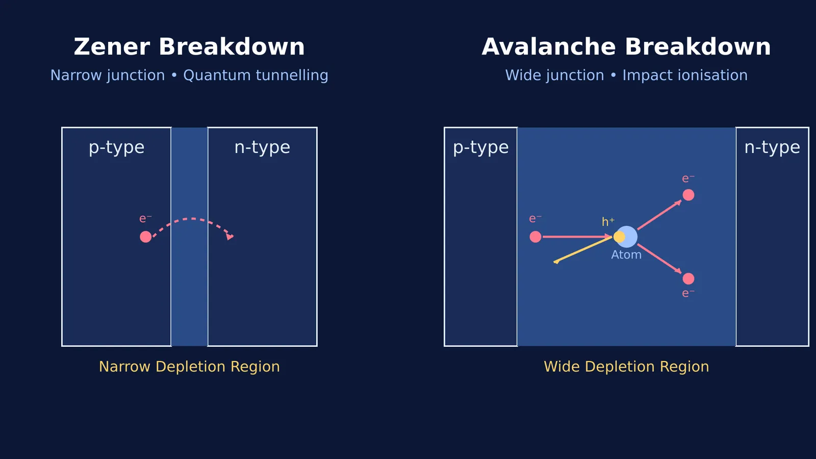
Zener breakdown occurs in highly doped p-n junctions. Because the doping concentration is high on both sides, the depletion region is squeezed into an extremely narrow layer.
When you apply a reverse voltage of less than 5V, the intense electric field across this tiny physical gap can reach approximately 3 × 10⁷ V/m (Wikipedia). This electric field is so concentrated that it provides enough force to literally rip electrons out of their covalent bonds.
Through a quantum mechanical process called field ionisation (or quantum tunnelling), electrons cross directly from the valence band on the p-side to the conduction band on the n-side. They pass through the potential barrier without needing to go over it. This sudden rush of electrons creates a sharp, rapid increase in current.
To brush up on semiconductor theory, the Fermi Concept Library can help you review definitions and visualise charge carriers inside these depletion regions.
Why does avalanche breakdown happen?
Avalanche breakdown takes place in lightly doped p-n junctions, which inherently have a much wider depletion region. Since the voltage spreads over a larger distance, the electric field is not strong enough to pull electrons directly across the bandgap.
Instead, the breakdown happens through a violent chain reaction. When a reverse voltage greater than 5V is applied (Wikipedia), the electric field accelerates the few existing minority carriers (electrons or holes) that naturally wander into the depletion zone. These carriers gain immense kinetic energy.
When these speeding carriers collide with atoms in the crystal lattice, they strike with enough force to knock bound electrons free, creating new electron-hole pairs. These newly freed carriers are immediately accelerated by the electric field and go on to collide with other atoms. This process, known as impact ionisation, multiplies the charge carriers exponentially, causing a massive "avalanche" of reverse current.
What is the difference between Zener and avalanche breakdown?
Here is a quick framework to tell the two mechanisms apart in textbook problems or lab experiments:
Doping concentration: The Zener effect occurs in heavily doped diodes; avalanche occurs in lightly doped ones.
Depletion region width: Zener breakdown relies on a very narrow depletion layer; avalanche breakdown requires a wider region so carriers have enough physical space to accelerate to high speeds.
Breakdown voltage: Zener breakdown typically triggers at lower voltages (below 5V). Avalanche breakdown triggers at higher voltages (above 5V).
Physical process: Zener is driven by quantum tunnelling (field ionisation) where no collisions are needed. Avalanche is driven by physical collisions (impact ionisation).
You can explore how altering doping concentration physically changes these layers by reviewing n-type and p-type semiconductors to see why depletion widths shrink or expand.
How does temperature change the breakdown voltage?
One of the most practical differences between the two breakdown mechanisms is how they react to environmental heat. This is crucial for answering exam questions and designing circuits.
The Zener breakdown voltage has a negative temperature coefficient. As the diode heats up, the semiconductor's internal energy bandgap slightly narrows. This physical change makes it even easier for electrons to tunnel across the gap, which means a lower reverse voltage is needed to trigger the breakdown.
Avalanche breakdown, conversely, has a positive temperature coefficient. When the ambient temperature increases, the atoms in the crystal lattice begin to vibrate more rapidly. These increased thermal vibrations act like a dense crowd, meaning the accelerated minority carriers collide with atoms much more frequently. Because they travel a shorter distance (a shorter mean free path) between collisions, they have less time to build up kinetic energy. Therefore, you must apply a higher voltage to give them enough energy to cause impact ionisation.
If you are struggling to remember how thermal energy interacts with these structures, you can read more about energy bands in conductors and insulators, or test your knowledge using the Fermi Problem Library to work through the logic step-by-step.
How do you identify the breakdown type in your diode?
If you are working with a circuit schematic or analysing a physics problem, use this checklist to determine which breakdown you are dealing with:
Check the rated voltage: Check the component's rated breakdown voltage (V_Z or V_BR). If it is less than 5V, it is operating via Zener breakdown (Wikipedia).
Above 6V rule: If the rated breakdown is greater than 6V, it is avalanche breakdown (Wikipedia). Many commercial "Zener diodes" rated at 9V or 12V are actually operating on the avalanche principle, despite their trade name.
Look for the doping descriptor: If a physics problem states the junction is heavily doped (p+ and n+), assume Zener breakdown.
Observe the temperature shift: If the required breakdown voltage drops when the component heats up, you are looking at the Zener effect. If the required voltage rises when hot, it is an avalanche diode.
This explains why diodes rated at approximately 5.6V are often chosen by engineers to create highly stable voltage references—at this specific point, the negative temperature coefficient of the Zener effect and the positive coefficient of the avalanche perfectly cancel each other out.