
On this page
It might seem like the simplest way to build a diode: take a block of p-type silicon, take a block of n-type silicon, and press them together.
But if you try this in a lab, you will just get two separate pieces of silicon. The interface will act as a resistor or an open circuit, not as a semiconductor junction.
To understand why, we have to look at the interface at the atomic level. The rules that govern macroscopic objects do not apply when we need electrons to cross from one crystal lattice to another.
Why does physical contact fail at the atomic scale?
For a p-n junction to work, charge carriers—electrons and holes—must be able to diffuse across the boundary. This initial diffusion creates the depletion region and the potential barrier that makes a diode function.
Diffusion requires a continuous, unbroken crystal lattice. When you simply press two crystals together, you break this continuity for two reasons:
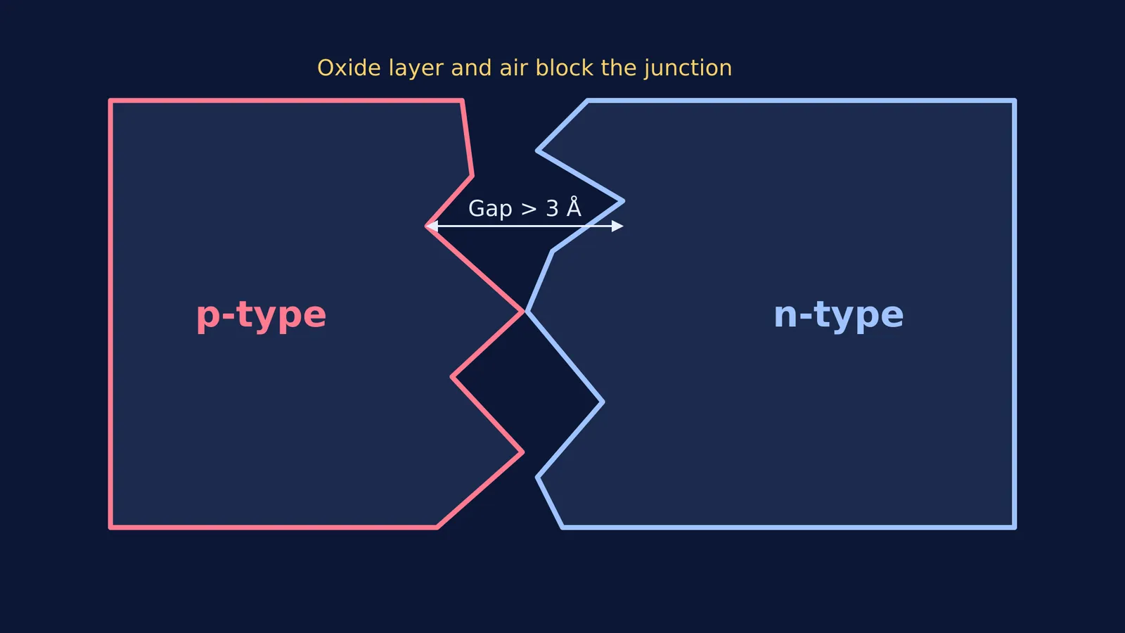
Surface roughness: No matter how smooth a surface looks or feels, it is rough on the atomic scale. According to the NCERT Class 12 Physics solutions, the inter-atomic spacing in a crystal is about 2 to 3 Å (0.2 to 0.3 nanometres). When you press two slabs together, the microscopic peaks on each surface touch, but they leave massive valleys and gaps everywhere else.
Lack of continuous bonds: Because the atoms across the gap are too far apart to form covalent bonds, the crystal lattice stops at the edge of each block. The charge carriers cannot "jump" across the empty space, meaning diffusion cannot happen.
When you practice with the Fermi Problem Library, you will notice that junction problems always assume a single, unbroken crystal structure. Without that continuous lattice, the equations for diffusion and drift currents do not apply because the carriers hit a physical wall.
Why is the native oxide layer a problem?
Even if you could somehow polish two surfaces perfectly flat at the atomic level, you would still face a chemical barrier before you could press them together.
When you expose a fresh silicon surface to air, it reacts with oxygen almost instantly. A native oxide layer (silicon dioxide) forms on the surface, growing to a thickness of about 1 nanometre (10 Å) within minutes or hours.
This oxide layer is an excellent electrical insulator. When you press the two oxidized crystals together, this insulating layer gets trapped in the middle, completely blocking the flow of charge carriers. Instead of a p-n junction, you have created a capacitor: two conductive plates separated by a dielectric.
How is a p-n junction actually made?
Because you cannot stitch two crystals together, a p-n junction must be fabricated within a single piece of semiconductor. Manufacturers use techniques that alter the atomic structure of a single wafer without breaking its crystal lattice.
Thermal diffusion
Instead of joining two blocks, manufacturers take a single wafer of, say, n-type silicon. They heat it in a furnace and expose one side to a gas containing p-type dopants, such as boron. The high temperature gives the boron atoms enough energy to diffuse into the crystal lattice, converting the top layer into p-type silicon.
Ion implantation
In modern fabrication, dopant atoms are accelerated to high speeds and fired directly into the silicon wafer. The atoms embed themselves into the crystal lattice. The wafer is then heated (annealed) to repair any damage to the lattice and activate the dopants.
Epitaxial growth
Sometimes, a new layer of silicon is grown directly on top of the existing wafer. The new atoms are deposited slowly so they align perfectly with the original lattice, continuing the crystal structure without interruption while adding different dopants.
How does physical contact compare to fabrication?
Here is a quick summary of why fabrication works and physical contact fails:
Lattice structure: Pressing leaves a discontinuous gap; fabrication maintains a single, continuous crystal.
Interface distance: Pressing leaves gaps much larger than 3 Å; fabrication keeps atoms at the correct 2 to 3 Å spacing.
Chemical purity: Pressing traps an insulating native oxide layer; fabrication happens in controlled environments to avoid oxides.
Result: Pressing creates an open circuit or a resistor; fabrication creates a functional diode.
Because the entire device remains one continuous crystal, there are no air gaps, no surface roughness, and no trapped oxide layers. The charge carriers can freely diffuse across the newly formed boundary, creating a working p-n junction.
If you are revising how energy levels shift across these junctions, you can read more about energy bands in conductors, semiconductors and insulators or look up n-type and p-type carrier concentration problems. For building a complete picture of semiconductor physics, explore the Fermi Concept Library.