
On this page
How do solar panels make electricity from sunlight?
A solar panel is made of many smaller units called solar cells, which rely on the photovoltaic effect. At the heart of almost every commercial solar cell is a silicon p-n junction, built from n-type and p-type semiconductors.
Silicon is a semiconductor, meaning it does not conduct electricity easily on its own. To change this, manufacturers add specific impurities in a process called doping. The top layer is usually n-type silicon, doped with phosphorus to provide extra free electrons. The bottom layer is p-type silicon, doped with boron to create "holes", which are missing electrons that act as positive charges.
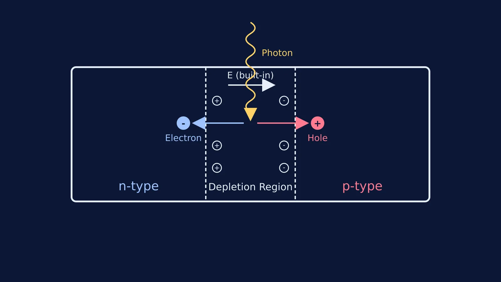
When these two layers meet, free electrons from the n-side diffuse into the p-side, leaving behind positively charged phosphorus ions. This creates a boundary known as the depletion region. The exposed ions set up a strong, built-in electric field pointing from the n-type side to the p-type side. This field acts as a barrier that stops more charges from crossing, and it is the invisible engine that drives the solar cell.
How does light free electrons?
When sunlight hits the panel, it delivers energy in packets called photons. If a photon has enough energy, it can knock an electron loose from a silicon atom.
This is the internal version of the photoelectric effect. Silicon has an energy gap of about 1.14 eV, distinguishing its energy bands from those of conductors and insulators. To free an electron, a photon must carry at least 1.14 eV of energy, which corresponds to wavelengths shorter than 1088 nm. Much of the sunlight reaching Earth has enough energy to do this.
When an electron is knocked free, it leaves behind a hole. Left alone, the electron and hole would quickly recombine and waste the energy as heat. But if this happens in or near the depletion region, the built-in electric field takes over. The field exerts a force that sweeps the negatively charged electron toward the n-side and the positively charged hole toward the p-side.
It can be hard to picture exactly how electric fields and charge carriers behave inside a crystal. The Fermi Simulation Lab provides interactive models where you can see how the built-in field separates the charges.
Why does the current flow?
As the built-in electric field pushes electrons into the n-type layer, they become trapped there. They cannot cross back because the electric field pushes them the other way.
This gathering of negative charges on the top layer and positive charges on the bottom creates a voltage difference. A standard single-junction silicon solar cell can produce a maximum open-circuit voltage of approximately 0.5 to 0.6 volts. Because this voltage is too low for most household uses, manufacturers wire many cells together in series so their voltages add up.
To use the energy, you connect a wire from the top n-type layer to an external circuit, and then back to the bottom p-type layer. The trapped electrons now have a path. They flow out through the wire, power a load like a lightbulb or a battery charger, and return to the p-side to recombine with the holes. Graphing this electrical behaviour produces characteristic solar cell I-V curves.
p-n junctions often feature in physics numericals. The Fermi Problem Library has a step-by-step solver that explains the reasoning behind semiconductor physics and the photoelectric effect.