
On this page
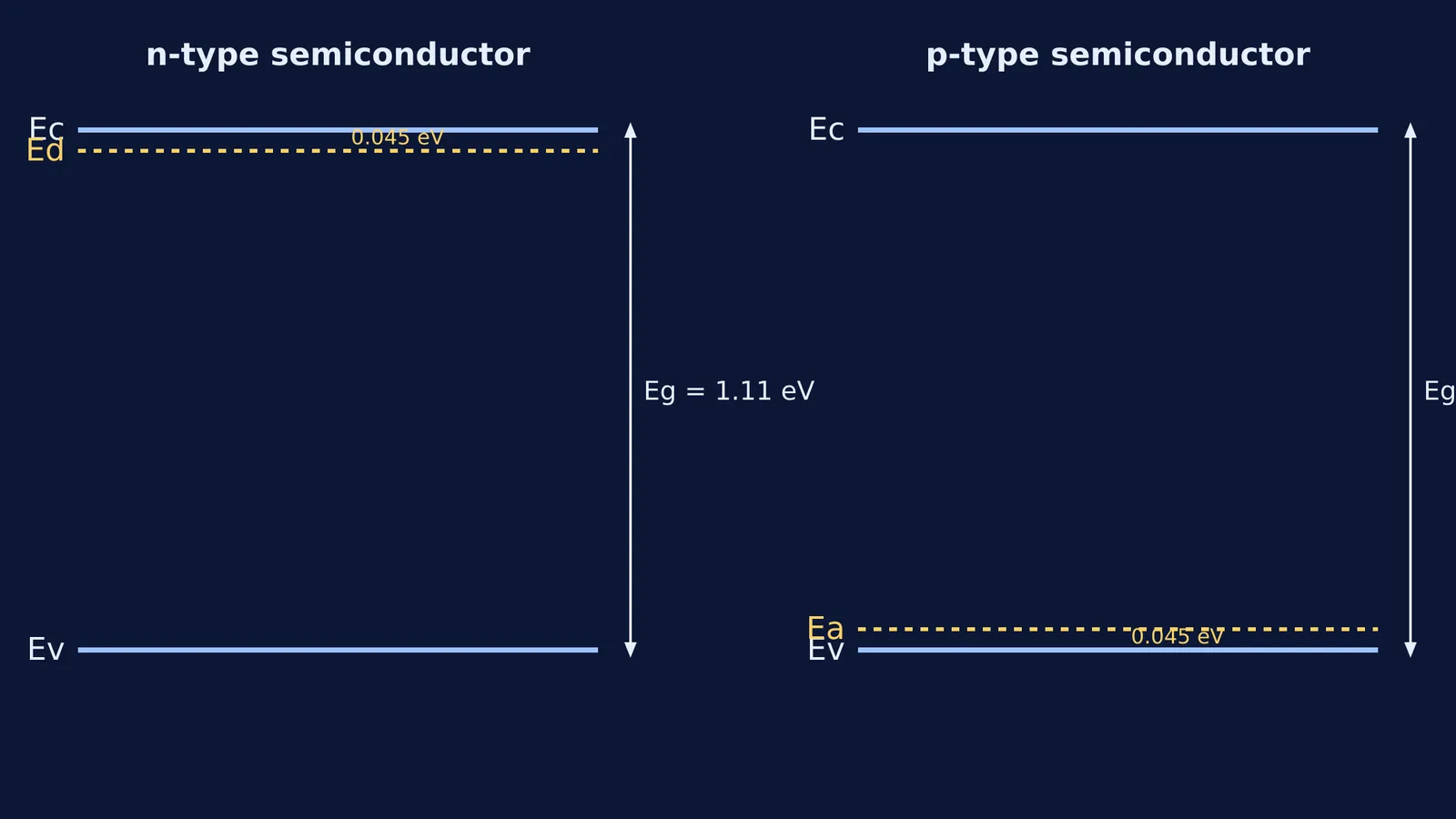
When you study intrinsic and extrinsic semiconductors, the most important tool is the energy band diagram. In a pure silicon crystal, the gap between the valence band (E_v) and the conduction band (E_c) is about 1.11 eV. But when we dope the crystal with impurities, we create new, shallow energy levels inside this forbidden gap.
Where these new levels sit explains why doped semiconductors conduct electricity so well, and why they respond strongly to small changes in temperature.
Where are the donor energy levels?
In an n-type semiconductor, we dope silicon with pentavalent atoms like phosphorus, arsenic or antimony. These atoms have five valence electrons. Four of them form strong covalent bonds with the neighbouring silicon atoms in the crystal lattice, but the fifth electron is left weakly bound to its parent atom.
On a band diagram, this fifth electron sits at the donor energy level (E_d), which is located just below the conduction band. The energy gap between the donor level and the conduction band is called the ionisation energy. According to HyperPhysics, the ionisation energy for phosphorus in silicon is just 0.045 eV.
Because this gap is so small, an electron sitting at the donor level needs very little energy to break free from the impurity atom and move into the conduction band. Once it reaches the conduction band, it is free to drift through the crystal and contribute to the electrical current.
If you are solving numericals on these populations, you can see how this affects the majority and minority carriers in our guide to n-type and p-type semiconductors: carrier concentration problems.
Where are the acceptor energy levels?
In a p-type semiconductor, we use trivalent impurities like boron, gallium or indium. With only three valence electrons, they cannot complete the four covalent bonds required by the silicon lattice. As a result, they leave a vacant spot—a hole—in the crystal structure.
These impurities introduce an acceptor energy level (E_a) just above the valence band. To create a mobile hole in the valence band, an electron from a nearby silicon atom must jump from the valence band up to the acceptor level to complete the bond. When this happens, the electron becomes trapped at the acceptor site, but it leaves behind a free hole in the valence band that can move and carry current.
The energy required for this jump is also tiny. For boron in silicon, the gap is exactly 0.045 eV. The electron only needs a slight nudge to reach the acceptor level.
This behaviour sets semiconductors apart from other materials. For a broader comparison, see our post on energy bands: conductors, semiconductors and insulators compared.
Why do they ionise so easily?
The key to understanding extrinsic semiconductors is that these impurity atoms are almost completely ionised at room temperature. But why does this happen so reliably?
At room temperature (300 K), the available thermal energy (kT) is about 0.026 eV. While 0.026 eV is slightly less than the 0.045 eV ionisation energy, statistical thermodynamics works in our favour. Because there are millions of empty states waiting in the conduction band, the statistical balance heavily favours the electrons making the jump.
The ambient heat of the room provides a constant, random vibration that easily knocks these weakly bound electrons into the conduction band, or bumps valence electrons up into the acceptor level to leave holes behind.
By contrast, the 1.11 eV main band gap is far too large for room-temperature heat to excite many electrons across it directly. Only a minuscule fraction of electrons can make the full jump from the valence band to the conduction band without the help of dopant levels.
How does the Fermi level shift?
When we add these donor or acceptor levels, we also change the overall balance of electrons and holes. This shifts the position of the Fermi level—the theoretical energy level where the probability of an electron occupying a state is exactly one-half.
In an intrinsic (pure) semiconductor, the Fermi level sits roughly in the middle of the band gap. However, when donor impurities are added to make an n-type semiconductor, the flood of new electrons in the conduction band pushes the Fermi level upwards, moving it closer to the conduction band. Conversely, in a p-type semiconductor, the abundance of holes in the valence band pulls the Fermi level downwards, closer to the valence band.
This shift in the Fermi level is crucial when joining p-type and n-type materials together to form a p-n junction, as the bands must bend to align the Fermi levels across the junction.
If you find it hard to picture how these electrons jump between energy levels, the Fermi Concept Library can help. Fermi's AI tutor can draw the band diagrams with you, checking your understanding as it goes, so you can build a clear mental model of semiconductor physics.